

Method for manufacturing gate structure
A gate structure and structure surface technology, which is applied in the field of semiconductor integrated circuit manufacturing technology, can solve problems such as impact, insufficient stability, and increased cost
- Summary
- Abstract
- Description
- Claims
- Application Information
AI Technical Summary
Problems solved by technology
Method used
Image

Examples
Embodiment Construction
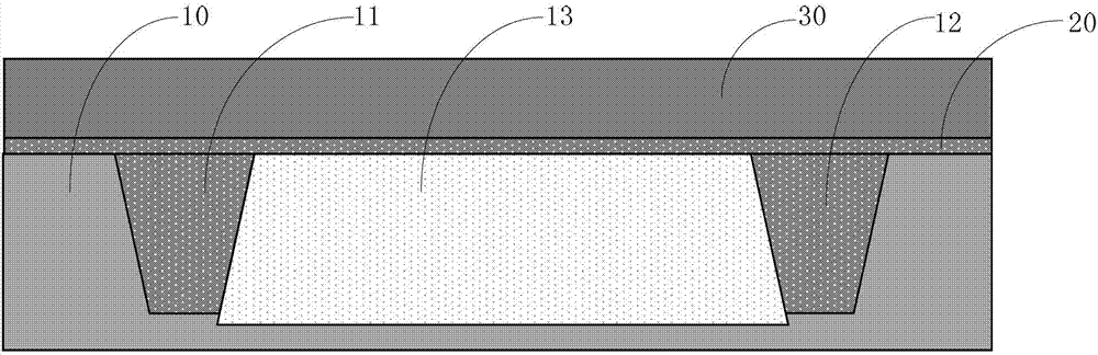
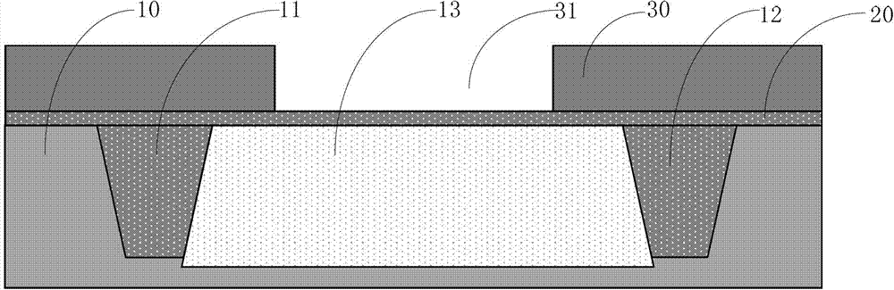
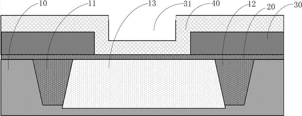
[0025] Figure 1-Figure 5 The process (cross-sectional view) of the method for fabricating a gate structure in Embodiment 1 of the present invention is shown.
[0026] see figure 1 ,
[0027] A substrate 10 is provided; a gate dielectric layer 20 is formed on the substrate 10 ; and a sacrificial layer 30 is deposited on the gate dielectric layer 20 .
[0028] The substrate 10 is a silicon substrate, and two device isolation layers 11 and 12 are formed in the substrate 10 . The two device isolation layers 11 , 12 are generally used to isolate the NMOS region and the PMOS region in the substrate 10 . The device isolation layer is formed by a shallow trench isolation (STI) method. A well 13 is formed between the two device isolation layers 11 , 12 .
[0029] The gate dielectric layer generally adopts oxide, nitride or oxynitride or composite. In this embodiment, silicon oxide is used for the gate dielectric layer 20 . Gate dielectric layer 20 is approximately 200 Angstroms...
PUM
| Property | Measurement | Unit |
|---|---|---|
| Thickness | aaaaa | aaaaa |
| Thickness | aaaaa | aaaaa |
Abstract
Description
Claims
Application Information