Chip welding method

A welding method and chip technology, which is applied in the field of chip welding and electronic parts welding, can solve the problems of low production efficiency, high price, and high price of unidirectional anisotropic conductive adhesive, so as to increase the product qualification rate, simplify the production process, and make up for equipment expensive effect

Inactive Publication Date: 2013-01-30
上海祯显电子科技有限公司
View PDF0 Cites 20 Cited by
  • Summary
  • Abstract
  • Description
  • Claims
  • Application Information

AI Technical Summary

Problems solved by technology

Although this process can achieve ultra-thin process requirements, its production equipment is special-purpose equipment, which is expensive and has low production efficiency, which is 1 / 3~1 / 5 of traditional surface mount equipment. Production requires a large investment in equipment to achieve
[0003] The price of the raw material unidirectional anisotropic conductive adhesive using the flip-down packaging process is expensive, and the performance of the product is greatly affected by external factors, such as ambient temperature, air dust, pressure and other conditions, which will cause changes in the welding effect, which has obvious potential for welding failure. risk

Method used


Image

  • Chip welding method
  • Chip welding method
  • Chip welding method

Examples


Embodiment 1

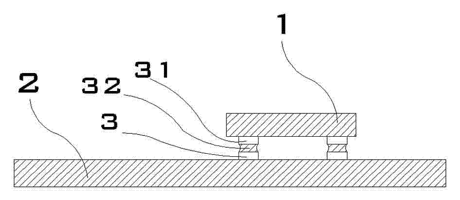
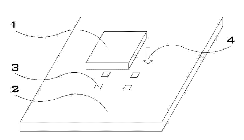
[0040] Such as figure 1 and figure 2 In the chip soldering structure diagram shown, first, the solder paste 32 is placed on the surface of the pad 3 of the epoxy resin substrate 2 through the stencil printing process, and then the pad 31 of the chip 1 is aligned with the pad 3 of the substrate 2 by a manipulator. , according to the direction of arrow 4, and then heat the substrate with chip 1 through a reflow oven to solidify the solder to complete the process of chip soldering; in this process, the amount of solder is selected according to the size of the pad, Subject to sufficient connection. In actual operation, it can be adjusted by selecting the thickness of the stencil and the size of the printing window. The thickness of the steel mesh can be selected from 20um to 200um.

[0041] In the process of heating and curing the solder in the reflow oven, different solders are selected according to the material of the substrate and the corresponding heating temperature is us...

Embodiment 2

[0051] Such as figure 1 with figure 2 As shown in the chip welding structure diagram, first, the silver paste 32 is placed on the surface of the pad 3 of the polyethylene terephthalate (PET) substrate 2 by automatic dispensing equipment, and then the pad 31 of the chip 1 is placed on the surface of the pad 3 of the chip 1 by a robot. Align the pad 3 of the substrate 2 and install it, stick it in the direction of the arrow 4, and then heat the substrate with the chip 1 through the reflow oven to solidify the solder to complete the chip soldering process; in this process, the solder The amount is selected according to the size of the pad, whichever can be fully connected. In actual operation, it can be adjusted by setting parameters such as the pressure of the dispensing equipment. The thickness of the conductive agent can be selected from 30um to 300um.

[0052] In the process of heating and curing the solder in the reflow oven, different solders are selected according to t...

Embodiment 3

[0062] Such as figure 1 with figure 2 As shown in the chip welding structure diagram, first, the conductive glue or non-conductive glue 32 is placed on the surface of the pad 3 of the polyimide (PI) substrate 2 through the automatic dispensing equipment, and then the pad 31 of the chip 1 is placed on the surface of the pad 31 of the chip 1 by a robot. The pad 3 of the quasi-substrate 2 is installed, and it is pasted according to the direction of the arrow 4, and then the position of the substrate chip on which the chip 1 is installed is locally pressurized and heated to solidify the solder, and the process of chip soldering is completed; in this process, the flux of the solder The amount is selected according to the size of the pad, whichever can be fully connected. In actual operation, it can be adjusted by setting parameters such as the pressure of the dispensing equipment.

[0063] In the process of pressurizing and heating the solder to solidify, it is realized by setti...


PUM


Abstract

The invention discloses a chip welding method. The chip welding method includes the steps of firstly, applying solder 32 to the surface of a pad 3 of a substrate 2; secondly, aligning a pad surface 31 of a chip 1 to the pad 3 of the substrate for mounting by a manipulator; thirdly, heating the chip with the chip well mounted to solidify the solder 32 by a reflow oven to complete chip welding. In certain cases, reinforcement is needed to make welding more reliable. The chip welding method is substitutive for traditional chip lead bonding and flip-chip packaging technology, production efficiency is improved, and production cost is decreased.

Description

technical field [0001] The invention relates to the field of electronic component welding, in particular to the field of chip welding, in particular to a chip welding method, which can be widely used in the fields of chip packaging, smart card packaging, electronic product assembly and the like. Background technique [0002] The application of surface mount technology has been widely used in today's electronic product assembly industry. It is a production technology with high production efficiency, universal equipment and high degree of automation. However, the components to be mounted are all components that have been packaged twice. The cost of component packaging is high, and the product volume is large. Especially in some applications such as smart card products that require small and ultra-thin requirements, it cannot be realized. . In order to achieve such application requirements, flip-packaging technology has emerged in the industry, that is, gold balls are made on ...

Claims


Application Information

Patent Timeline
Patent Type & Authority Applications(China)
IPC IPC(8): H01L21/60H05K3/34
CPCH01L2224/16225
Inventor 陆红梅
Owner 上海祯显电子科技有限公司
Why Eureka
Try Eureka