ITO Sputtering Target
A technology of sputtering target and backing plate, applied in the field of ITO sputtering target, which can solve the problems of inability to melt and inject gaps, different electrical characteristics, etc.
- Summary
- Abstract
- Description
- Claims
- Application Information
AI Technical Summary
Problems solved by technology
Method used
Image
Examples
Embodiment 1)
[0053] As a raw material, the specific surface area is 5m 2 The mixed powder obtained by mixing the indium oxide powder and tin oxide powder in a weight ratio of 9:1 per gram is mixed and pulverized by a wet medium agitation mill based on a ball mill, and then injected into a die, at a rate of 700kg / cm 2 pressure forming to produce ITO molded body.
[0054] Then, the ITO molded body was heated from room temperature to 1500° C. at a rate of 5° C. / min in an oxygen atmosphere, then kept at 1500° C. for 20 hours, and then furnace-cooled and sintered.
[0055] The surface of the sintered body thus obtained was ground to a thickness of 6.5 mm using No. 400 diamond abrasive grains on a surface grinder, and the side was cut into a size of 127 mm×508 mm with a diamond cutter to obtain an ITO target member. Make two such processed bodies.
[0056] These sintered bodies were placed on a hot plate set at 200° C., and after the temperature was raised, indium was attached to only the side...
Embodiment 2)
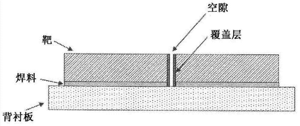
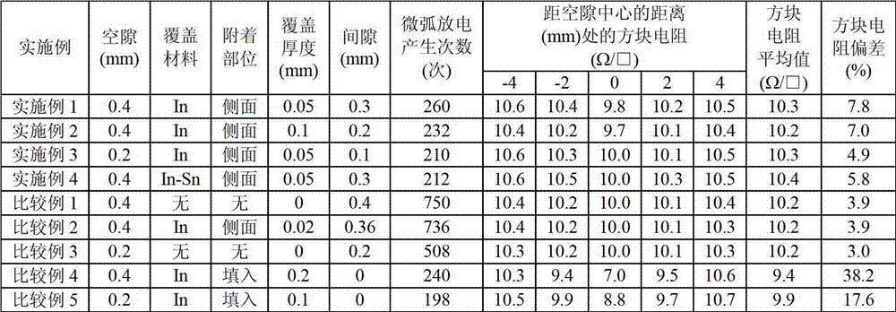
[0068] It carried out under the same conditions as Example 1 except having changed the thickness of a cover layer into 0.1 mm. The result is similarly shown in Table 1, figure 1 shown. The distance (interval) between the covering layers of adjacent divided targets was 0.2 mm.
[0069] The number of occurrences of micro-arcs was 232 times, the average value of the square resistance was 10.2Ω / □, and the deviation of the square resistance was 7.0%. The result was that the square resistance was a moderate value, the deviation of the square resistance was small, and the number of occurrences of micro-arcs was small. .
[0070] In the case of ITO, the properties of the film on the substrate can be evaluated by the sheet resistance, and the small variation in the sheet resistance means that the film is formed uniformly on the substrate.
Embodiment 3)
[0072] It carried out under the same conditions as Example 1 except having changed the gap into 0.2 mm. The distance (interval) between the covering layers of adjacent divided targets was 0.1 mm. The result is also shown in Table 1, figure 1 shown.
[0073] The number of occurrences of micro-arcs was 210 times, the average value of sheet resistance was 10.3Ω / □, and the variation of sheet resistance was 4.9%. The result was that the sheet resistance was moderate, the variation of sheet resistance was small, and the number of occurrences of micro-arcs was small. .
[0074] In the case of ITO, the properties of the film on the substrate can be evaluated by the sheet resistance, and the small variation in the sheet resistance means that the film is formed uniformly on the substrate.
PUM
| Property | Measurement | Unit |
|---|---|---|
| thickness | aaaaa | aaaaa |
| thickness | aaaaa | aaaaa |
| thickness | aaaaa | aaaaa |
Abstract
Description
Claims
Application Information


