Method for preparing ordered array of metal nano-particles with adjustable space and appearance
A technology of metal nanoparticles and ordered arrays, applied in nanostructure manufacturing, nanotechnology for materials and surface science, nanotechnology, etc., can solve the problem that the preparation method of nanoparticle arrays is not suitable for industrial production, and achieve decorative effects Good, low energy consumption, strong metallic effect
- Summary
- Abstract
- Description
- Claims
- Application Information
AI Technical Summary
Problems solved by technology
Method used
Image

Examples
Embodiment 1
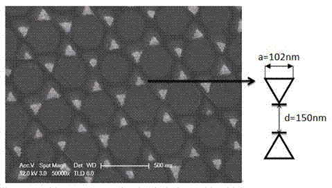
[0047] In an oxygen atmosphere of 10 Pa, adjust the power of the plasma cleaning machine to 30 W, clean the surface of the single crystal silicon substrate for 30 min, and take out the substrate; use the liquid surface self-assembly method to uniformly spread a layer of 460nm layer of polystyrene nanospheres. In an oxygen atmosphere of 10 Pa, the power of the plasma cleaner was adjusted to 30 W, and the silicon substrate covered with polystyrene nanosphere layer was etched for 1 min with the plasma cleaner.
[0048] Using the etched polystyrene nanosphere layer as a template, a vacuum coating machine was used in 2×10 -3 Under the vacuum degree of Pa, 10 nm of cadmium was first deposited on the surface of the polystyrene nanosphere layer template, and then 30 nm of gold was deposited, and the deposition rate was 3 nm·min. -1, forming a cadmium-gold film. The self-assembled layer of polystyrene nanospheres was dissolved in chloroform solution, washed with absolute ethanol and...
Embodiment 2
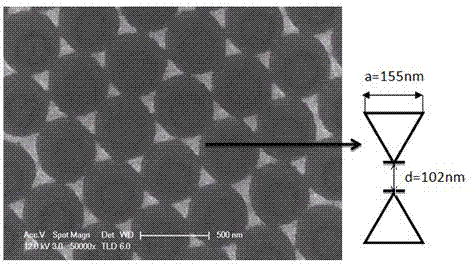
[0051] In an oxygen atmosphere of 10 Pa, adjust the power of the plasma cleaning machine to 30 W, clean the surface of the single crystal silicon substrate for 30 min, and take out the substrate; use the liquid surface self-assembly method to uniformly spread a layer of diameter 460 nm layer of polystyrene nanospheres. In an oxygen atmosphere of 10 Pa, the power of the plasma cleaner was adjusted to 30 W, and the silicon substrate covered with polystyrene nanosphere layer was etched for 2 min with the plasma cleaner.
[0052] Using the etched single-layer polystyrene nanometer as a template, a vacuum coating machine was used in 2×10 -3 Under the vacuum degree of Pa, 10 nm of cadmium was first deposited on the surface of the polystyrene nanosphere layer template, and then 30 nm of gold was deposited, and the deposition rate was 3 nm·min. -1 , forming a cadmium-gold film. The self-assembled layer of polystyrene nanospheres was dissolved in chloroform solution, washed with abs...
Embodiment 3
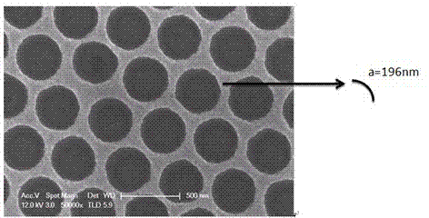
[0055] In an oxygen atmosphere of 10 Pa, adjust the power of the plasma cleaning machine to 30 W, clean the surface of the single crystal silicon substrate for 30 min, and take out the substrate; use the liquid surface self-assembly method to uniformly spread a layer of 460 nm layer of polystyrene nanospheres. In an oxygen atmosphere of 10Pa, the power of the plasma cleaner was adjusted to 30W, and the silicon substrate covered with polystyrene nanospheres was etched for 5 min with the plasma cleaner.
[0056] Using the etched single-layer polystyrene nanosphere layer as a template, a vacuum coating machine was used in 2×10 -3 Under the vacuum degree of Pa, 10 nm of cadmium was first deposited on the surface of the polystyrene nanosphere layer template, and then 30 nm of gold was deposited, and the deposition rate was 3 nm·min. -1 , forming a cadmium-gold film. The self-assembled layer of polystyrene nanospheres was dissolved in a chloroform solution, washed with absolute e...
PUM
| Property | Measurement | Unit |
|---|---|---|
| Diameter | aaaaa | aaaaa |
| Diameter | aaaaa | aaaaa |
Abstract
Description
Claims
Application Information
 - R&D
- Intellectual Property
- Life Sciences
- Materials
- Tech Scout
- Unparalleled Data Quality
- Higher Quality Content
- 60% Fewer Hallucinations
Browse by: Latest US Patents, China's latest patents, Technical Efficacy Thesaurus, Application Domain, Technology Topic, Popular Technical Reports.
© 2025 PatSnap. All rights reserved.Legal|Privacy policy|Modern Slavery Act Transparency Statement|Sitemap|About US| Contact US: help@patsnap.com