Method for growing silicon carbide mono-crystals through multi-crucible physical vapor transport technology, and device thereof

A technology of physical vapor transport and silicon carbide single crystal, which is applied in the growth of polycrystalline materials, chemical instruments and methods, single crystal growth, etc., can solve the problems of inconspicuous advantages and increased energy consumption, so as to improve growth efficiency and reduce The effect of production costs

Active Publication Date: 2013-02-13
李汶军 +1
View PDF10 Cites 23 Cited by
  • Summary
  • Abstract
  • Description
  • Claims
  • Application Information

AI Technical Summary

Problems solved by technology

For example, the Chinese Invention Patent No. 200910238110.0 applied for on 2009.11.18 discloses a technology for growing silicon carbide crystals by physical vapor transport. This technology places silicon carbide seed crystals on the top of the crucible and silicon carbide raw materials on the bottom of the crucible. However, one Only one silicon carbide single crystal can be grown in the single crystal furnace
The Chinese invention patent No. 201010152392.5 applied on April 20, 2010 has made further improvements on the basis of the above. This technology places silicon carbide seed crystals at the bottom of the crucible, and silicon carbide raw materials at the top of the crucible. However, a single crystal furnace using this technology can only grow a silicon carbide crystal
However, for the growth of silicon carbide single crystal, due to the high growth temperature, close to 2300°C, the top view structure of the furnace is circular instead of rectangular. Although it can be achieved by using the left and right multi-crucible growth technology described in the above patent It is possible to grow multiple silicon carbide crystals in one furnace at the same time, but since several crucibles are placed at the bottom of the furnace at the same time, a larger size furnace is bound to be required, so that the energy consumption per unit time of the furnace is greatly increased, which is different from the traditional increase in crystal size Compared with the method, the advantage of this method is not obvious

Method used


Image

  • Method for growing silicon carbide mono-crystals through multi-crucible physical vapor transport technology, and device thereof
  • Method for growing silicon carbide mono-crystals through multi-crucible physical vapor transport technology, and device thereof
  • Method for growing silicon carbide mono-crystals through multi-crucible physical vapor transport technology, and device thereof

Examples


Embodiment 1

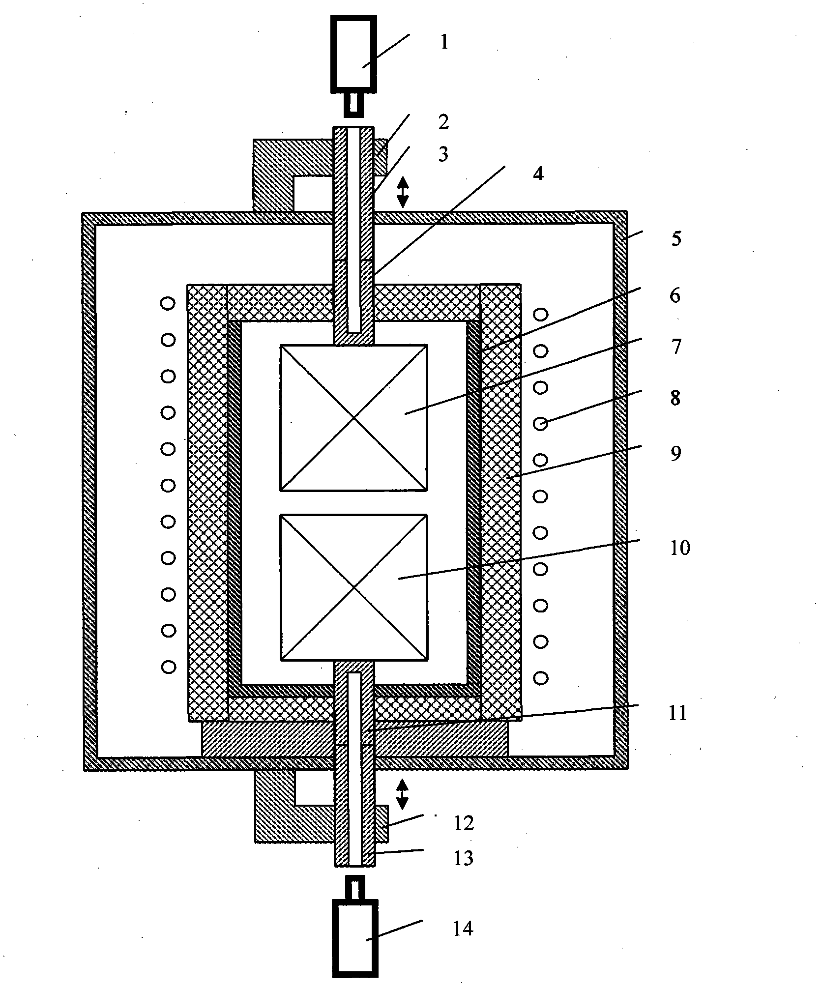
[0026] figure 1 Shown is a schematic diagram of the device structure for growing silicon carbide single crystals by double-crucible physical vapor transport technology. In this device, the graphite heating element 6 is wrapped in the insulating material 9, the induction coil 8 is located outside the insulating material 9, and the two graphite crucibles 7 and 10 arranged up and down are located in the furnace formed by the graphite heating element 6 and the insulating material 9. , the upper crucible 7 is suspended on the lifting rod 3 through the upper temperature measuring tube 4, and the lower crucible 10 is placed upside down on the lowering rod 13 through the lower temperature measuring tube 11. The temperature of the upper and lower crucibles is determined by the main temperature control device and the secondary temperature control device. The temperature control device includes infrared thermometer 1 or 14, Eurotherm temperature control meter and intermediate frequency p...

Embodiment 2

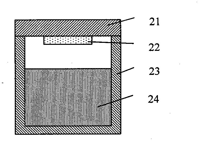
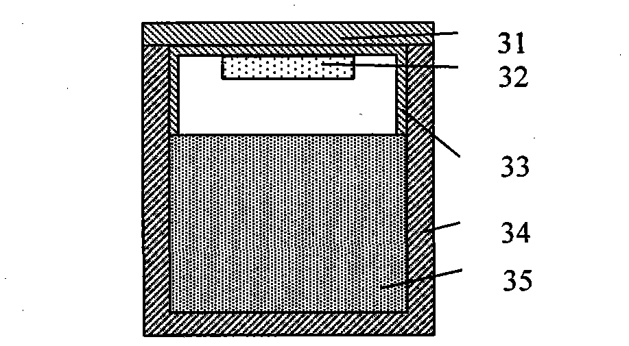
[0028] Taking the growth of silicon carbide single crystal by double-crucible physical vapor transport technology as an example, this embodiment adopts figure 1 The device structure shown, figure 2The upper crucible structure shown and the lower crucible structure shown in Fig. 3(a). In the upper crucible, high-purity silicon carbide powder is used as the raw material for growth, and in the lower crucible, high-purity silicon carbide powder is used as the raw material, and the polycrystalline silicon carbide block obtained by sintering in argon at 1800°C for 5 hours is used as the growth raw material. The process is as follows: respectively place a certain amount of high-purity silicon carbide powder and silicon carbide polycrystalline block in the upper and lower graphite crucibles, tighten the upper crucible cover with the silicon carbide seed crystal attached, so that the gap between the raw material and the seed crystal in the upper crucible The distance between them is ...

Embodiment 3

[0030] Embodiment 3 adopts figure 1 The device structure shown and figure 2 For the structure of the upper crucible shown and the structure of the lower crucible shown in Figure 3(b), the temperature measured by the upper crucible is used as the main control temperature. Compared with Example 2, the temperature control method and process parameters remain the same, but the selected lower crucible structure is different. Embodiment 2 adopts the lower crucible structure shown in FIG. 3( a ), and this embodiment adopts the lower crucible structure shown in FIG. 3( b ). From the size of the silicon carbide crystal obtained by above method and device (as Figure 5(a) and 5(b) ), the silicon carbide crystal grown in the upper crucible has a diameter of 60 mm and a thickness of 21-23 mm. The silicon carbide crystal grown in the lower crucible has a diameter of 65 mm and a thickness of 12-13 mm.


PUM

PropertyMeasurementUnit
diameteraaaaaaaaaa
thicknessaaaaaaaaaa
thicknessaaaaaaaaaa

Abstract

The invention discloses a method for growing silicon carbide mono-crystals through a multi-crucible physical vapor transport technology, and a device thereof. The device is characterized in that the multi-crucible growth technology is adopted in the growth process of the silicon carbide mono-crystals, two graphite crucibles arrayed in a top-bottom manner are simultaneously placed in the graphite heating unit of a hearth, the upper crucible is suspended on a lifting rod, the lower crucible is inversely placed on a falling rod, two seed crystals are positioned at two ends of the graphite heating unit in a low temperature zone, a raw material is positioned in the middle of the graphite heating unit in a high temperature zone, and the temperatures of the upper crucible and the lower crucible are determined by a master temperature controller and a secondary temperature controller. The silicon carbide crystals growing though adopting the method have the advantages of high production efficiency and low production cost, so the method is suitable for the large-scale growth of the mono-crystals.

Description

technical field [0001] The present invention relates to a method and device for growing silicon carbide crystals, in particular to a method and device for growing silicon carbide single crystals using multi-crucible physical vapor transport technology. The silicon carbide single crystals grown by this method have high production efficiency and low production cost. Suitable for large-scale single crystal growth. Background technique [0002] At present, the rapid development of the semiconductor industry has once again stimulated the innovation of modern science and technology. As a third-generation wide-bandgap semiconductor material, silicon carbide is superior to commonly used substrate materials in terms of thermal, electrical, and corrosion resistance, and can be widely used in the manufacture of semiconductor devices such as semiconductor lighting, microelectronics, and power electronics. In the past few decades, a variety of high-performance silicon carbide-based semi...

Claims


Application Information

Patent Timeline
Patent Type & Authority Applications(China)
IPC IPC(8): C30B23/00C30B29/36
Inventor 李汶军李根法
Owner 李汶军
Why Eureka
Try Eureka