B4-flash device and manufacture method thereof

A manufacturing method and device technology, which is applied in semiconductor/solid-state device manufacturing, electric solid-state devices, semiconductor devices, etc., can solve the problems of limiting gate length, etc., and achieve the effects of improving performance, reducing the remaining hole volume, and saving costs

Active Publication Date: 2013-02-20
SHANGHAI HUALI MICROELECTRONICS CORP
View PDF3 Cites 2 Cited by
  • Summary
  • Abstract
  • Description
  • Claims
  • Application Information

AI Technical Summary

Problems solved by technology

Although this substrate-bias-assisted band-to-band p-channel device has also been reported before, however, in order to obtain enough hot electrons to compile, a high drain voltage is still required, and an excessive drain voltage will make Channel penetration is easy, which limits the gate length (T.Ohnakado, et al., IEEE Trans. EL, Vol.46, No.9, 1999, pp.1866-1870.), which also limits the size of the device reduce

Method used


Image

  • B4-flash device and manufacture method thereof
  • B4-flash device and manufacture method thereof
  • B4-flash device and manufacture method thereof

Examples


Embodiment Construction

[0020] The present invention will be explained in detail below in conjunction with the accompanying drawings.

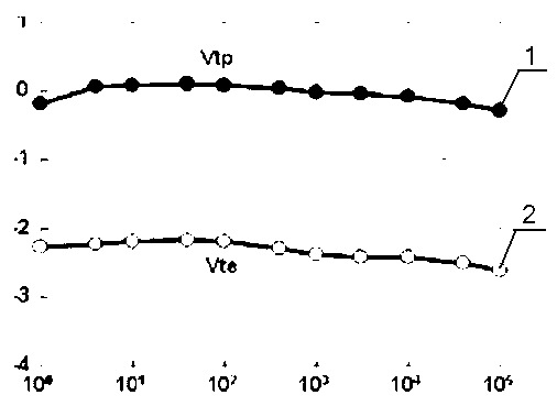
[0021] For the 60nm SONOS structure, the substrate bias assisted band to band tunneling-induced hot electron injection (Bulk Bias assisted Band to Band induced hot electron injection) is used to compile, and the hole tunneling injection of FN is used to achieve erasure. Compared with other structures, it has many advantages. Both electrons and holes act on the silicon oxide layer during its cycle, but the programming and erasing voltages still vary periodically. Such as figure 2 As shown in , wherein, line segment 1 and line segment 2 represent the change of the ordinate voltage of programming and erasing with the side length of the abscissa cycle. It can be seen from the figure that the trend of compiling and erasing states decreases at the same time (the actual required voltage gradually increases). Since the operating window does not change significantly, it me...


PUM

PropertyMeasurementUnit
thicknessaaaaaaaaaa
thicknessaaaaaaaaaa

Abstract

The invention provides a B4-flash device and a manufacture method thereof. The B4-flash device comprises a substrate, a first silicon oxide layer, a silicon nitride layer and a second silicon oxide layer, wherein the first silicon oxide layer, the silicon nitride layer and the second silicon oxide layer are sequentially installed on the substrate, the first silicon oxide layer comprises a first section, a second section and a third section which are sequentially distributed along a channel direction, and the thickness ratio of the first section, the second section and the third section is 1.5-2.5:0.8-1.2:1.5-2.5. An embodiment of the B4-flash device remits degeneration of silicon oxide and influences of electronic local area injection compiling and hole uniformity injection wiping through a heterogeneous silicon oxide structure so as to increase reliability of the device.

Description

technical field [0001] The invention relates to a device and a manufacturing method thereof, in particular to a device suitable for B4-flash compilation and hole tunneling injection and erasing and a manufacturing method thereof. Background technique [0002] For NOR flash memory cells, the most important limit to the continued reduction in size is the shortening of the gate length. This is mainly because the channel thermal electron (CHE) injection compilation method requires a certain voltage at the drain terminal, and this voltage has a great influence on the penetration of the source and drain terminals. For short channel devices, the channel thermal electron (CHE) method Not applicable. Another problem is that this limits the compilation yield of NOR flash compared to NAND and AND data storage devices. [0003] Recently, Shoji Shukuri et .al proposed a novel P-channel memory cell ("60nm NOR Flash Memory Cell Technology Utilizing Back Bias Assisted Band-to-Band Tunnel...

Claims


Application Information

Patent Timeline
Patent Type & Authority Applications(China)
IPC IPC(8): H01L27/115H01L21/8247
CPCG11C16/0466G11C16/04H01L29/792H01L21/28282H01L29/40117
Inventor 田志顾经纶
Owner SHANGHAI HUALI MICROELECTRONICS CORP
Why Eureka
Try Eureka