Two-dimensional electronic material device and mixed photoetching method thereof

A two-dimensional electronic and mixed light technology, applied in circuits, electrical components, electrical solid devices, etc., can solve the problems of mobility degradation of two-dimensional electronic materials, destruction of intrinsic properties of two-dimensional electronic materials, and impact on device performance, etc. Improve lithography accuracy, save processing time, and achieve the effect of high lithography accuracy

Active Publication Date: 2015-04-15
TSINGHUA UNIV
View PDF3 Cites 0 Cited by
  • Summary
  • Abstract
  • Description
  • Claims
  • Application Information

AI Technical Summary

Problems solved by technology

[0004] In the above-mentioned devices, the two-dimensional electronic material is first laid directly on the substrate, and the gate dielectric, gate-source-drain electrodes, etc. are also formed on it during the preparation process. These processes will cause the intrinsic characteristics of the two-dimensional electronic material to be affected. For example, the mobility of two-dimensional electronic materials may be degraded, and the destruction of the intrinsic properties of two-dimensional electronic materials will affect the performance of the entire device.

Method used


Image

  • Two-dimensional electronic material device and mixed photoetching method thereof
  • Two-dimensional electronic material device and mixed photoetching method thereof
  • Two-dimensional electronic material device and mixed photoetching method thereof

Examples


Embodiment Construction

[0034] Embodiments of the present invention will be described below with reference to the drawings. Elements and features described in one drawing or one embodiment of the present invention may be combined with elements and features shown in one or more other drawings or embodiments. It should be noted that representation and description of components and processes that are not related to the present invention and known to those of ordinary skill in the art are omitted from the drawings and descriptions for the purpose of clarity.

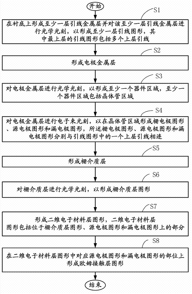
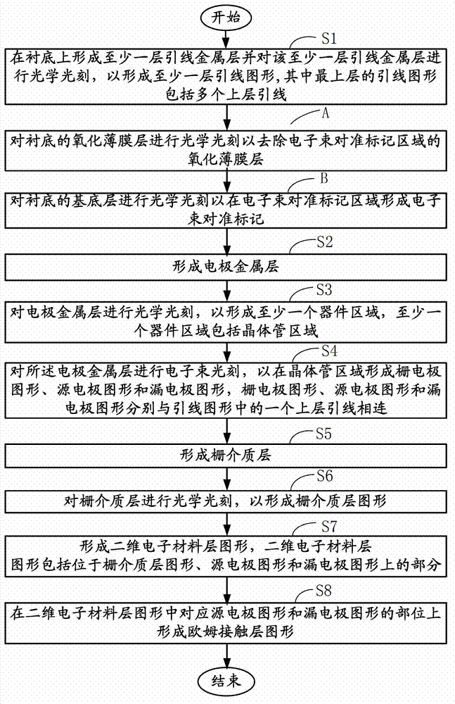
[0035] refer to figure 1 , the present invention provides a hybrid photolithography method for a two-dimensional electronic material device, an embodiment of which includes the following steps:

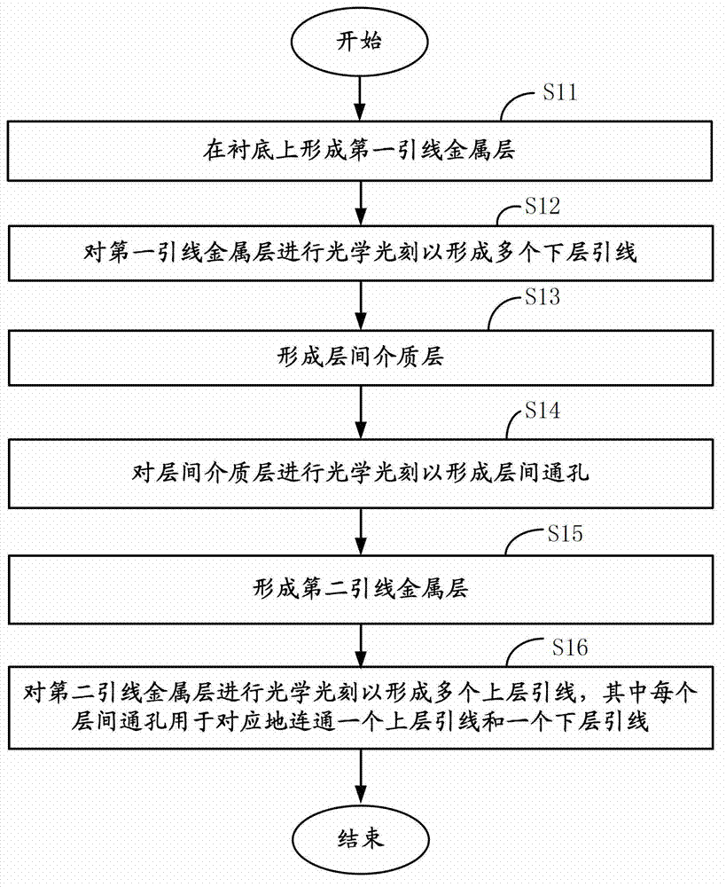
[0036] Step S1: forming at least one lead metal layer on the substrate and performing photolithography on the at least one lead metal layer to form at least one layer of lead pattern, wherein the uppermost lead pattern includes a plurality of upper layer ...


PUM

PropertyMeasurementUnit
thicknessaaaaaaaaaa
thicknessaaaaaaaaaa

Abstract

The invention relates to a two-dimensional electronic material device and a mixed photoetching method thereof, wherein the method comprises the following steps: forming at least one lead metal layer on a substrate, and performing optical photoetching on the at least one lead metal layer so as to form at least one layer of lead figures, wherein an uppermost layer comprises a plurality of upper layer leads, and a grid electrode, a source electrode and a drain electrode are respectively connected with one upper layer lead; forming an electrode metal layer; performing the optical photoetching on the electrode metal layer so as to form a transistor region; performing electron-beam photoetching on the electrode metal layer so as to form the figures of the grid electrode, the source electrode and the drain electrode; forming a grid dielectric layer; performing the optical photoetching on the grid dielectric layer so as to form the figure of the grid dielectric layer; forming the figure of a two-dimensional electronic material layer; and forming the figure of an ohmic contact layer. The device is capable of eliminating or decreasing the destruction of intrinsic properties of the two-dimensional electronic material, capable of greatly improving the photoetching precision of small-size devices based on guaranteeing the process cost and improving the performance of the devices, and capable of saving the processing time based on guaranteeing the processing precision.

Description

technical field [0001] The invention relates to the field of semiconductors, in particular to a two-dimensional electronic material device and a hybrid photolithography method thereof. Background technique [0002] Two-dimensional electronic materials with a single-layer sheet structure composed of carbon atoms, such as graphene, are available due to their ultra-high intrinsic carrier mobility, ultra-high strong-field drift velocity, and extremely high current-carrying capacity. To prepare a new generation of semiconductor devices with smaller size and faster conduction speed. [0003] The existing two-dimensional electronic material device includes a substrate on which a two-dimensional electronic material is formed, and the two-dimensional electronic material is used as a channel material of a semiconductor device, and a source / drain electrode and a gate dielectric (gate oxide layer) are sequentially formed on it. and gate electrodes. [0004] In the above-mentioned devi...

Claims


Application Information

Patent Timeline
Patent Type & Authority Patents(China)
IPC IPC(8): H01L21/027H01L21/28H01L29/423H01L29/417H01L23/48H01L21/48
Inventor 吴华强肖柯吕宏鸣钱鹤伍晓明
Owner TSINGHUA UNIV
Why Eureka
Try Eureka