Orthohexagonal crystal silicon solar wafer and solar battery manufactured thereby

A technology of solar silicon wafers and solar cells, which is applied in circuits, electrical components, semiconductor devices, etc., can solve the problems of reducing the output power of a single cell, not improving the utilization rate of silicon rods, and the effective area of ​​​​the cell is small, so as to reduce the return to the furnace Volume, area increase, effect of increasing area

Inactive Publication Date: 2013-02-27
JA SOLAR
View PDF3 Cites 8 Cited by
  • Summary
  • Abstract
  • Description
  • Claims
  • Application Information

AI Technical Summary

Problems solved by technology

In the process of squaring, the excised part is used as the scrap material, which usually accounts for 15%-30% of the crystal silicon rod. At present, the processing of the scrap scrap is usually done by returning to the furnace and re-drawing. In fact, this This method increases the amount of reheating, which is a waste in disguise
[0004] China Utility Model Authorized Patent (Patent No. 201020032032.7) discloses a technical solution for cutting the finished solar cells to make regular hexagonal cells. However, this technical solution has the foll...

Method used


Image

  • Orthohexagonal crystal silicon solar wafer and solar battery manufactured thereby
  • Orthohexagonal crystal silicon solar wafer and solar battery manufactured thereby
  • Orthohexagonal crystal silicon solar wafer and solar battery manufactured thereby

Examples


Embodiment 1

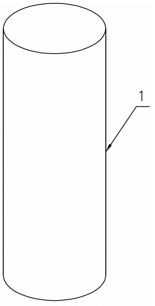
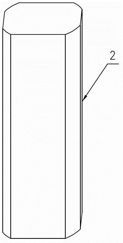
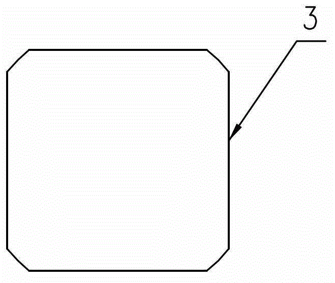
[0029] Such as Figure 5-7 As shown, it is a regular hexagonal crystalline silicon solar silicon wafer of the present invention, including a silicon wafer. The resulting sheet. In this embodiment, the regular hexagonal silicon wafer 5 is cut into regular hexagonal columns 6 along the axial direction of the inscribed regular hexagon of the cross section of the cylindrical silicon rod 1 , and then sliced. Specifically, the crystalline silicon rod 1 with a cross-sectional diameter of 200 mm is square cut into a regular hexagonal column 6 with a side length of 100 mm, and then the regular hexagonal column 6 is sliced ​​to form a regular hexagonal silicon wafer 5 . The cut-off scrap of the crystalline silicon rod is greatly reduced, the utilization rate of the crystalline silicon rod is improved, the amount of returning to the furnace is reduced, and the production cost is saved.

[0030] A solar cell made of the regular hexagonal crystalline silicon solar silicon wafer. The reg...

Embodiment 2

[0032] The crystalline silicon rod with a cross-sectional diameter of 165mm is square cut into a regular hexagonal column with a side length of 82.5mm. After slicing, the regular hexagonal silicon wafer undergoes texturing, diffusion, plasma etching, and chemical vapor deposition to reduce reflection. Film, screen printing paste, sintering process to make a regular hexagonal solar cell, solar cell side length 82.5mm, effective area 17683mm 2 .

[0033] Compared with quasi-square silicon wafers and batteries, regular hexagonal silicon wafers and batteries, the edge material cutting loss of crystal silicon rods is reduced by 5-15%, the area of ​​silicon wafers and batteries is increased by 5-15%, and the battery power is increased by 5- 15%. For example, for silicon wafers and batteries made of 6.5' crystalline silicon rods, the utilization rate of quasi-square silicon wafers to crystalline silicon rods is 72.4%, and the utilization rate of regular hexagonal silicon wafers to c...


PUM


Abstract

The invention discloses an orthohexagonal crystal silicon solar wafer, which comprises an orthohexagonal silicon wafer, and the orthohexagonal silicon wafer is a sheet body formed by an inscribed regular hexagon of the cross section of a cylindrical crystal silicon rod. The invention also discloses a solar battery manufactured by the orthohexagonal crystal silicon solar wafer, and the orthohexagonal silicon wafer is manufactured into an orthohexagonal solar battery by adopting the manufacture process of a crystal silicon solar battery. The silicon wafer is orthohexagonal, so that the cut-off flaw-piece materials of the crystal silicon rod are greatly reduced, the utilization ratio of the crystal silicon rod is improved, the return quantity is reduced and the manufacturing cost is saved. The orthohexagonal solar battery has increased effective area and improved output power, realizes seamless splicing of battery components manufactured into the battery and the limited arrangement area of the components as far as possible, and satisfies the requirement for welding the battery components.

Description

technical field [0001] The invention relates to the technical field of photovoltaic utilization of crystalline silicon solar energy, in particular to a regular hexagonal crystalline silicon solar wafer and a solar cell made of the silicon wafer. Background technique [0002] In the manufacturing process of crystalline silicon solar silicon wafers and batteries, silicon is first made into cylindrical crystalline silicon rods by Czochralski or zone melting methods. In order to improve the efficiency of solar cell modules, silicon wafers need to cover the entire module area as much as possible. Therefore, the crystalline silicon rods also need to be made into rounded square silicon chips with a thickness of 150-200 μm through processes such as square rooting and slicing. The outer contour of each silicon chip is composed of four straight sides and rounded corners, commonly known as quasi-square. , Quasi-square silicon wafers are directly used to make solar cells, and then solar...

Claims


Application Information

Patent Timeline
IPC IPC(8): H01L31/0352C30B29/06
Inventor 杨伟强黄旭光魏红军宋倩倩
Owner JA SOLAR
Why Eureka
Try Eureka