

Longitudinal NPN triggered high-voltage ESD protective device with high maintaining voltage
A high sustain voltage and ESD protection technology, applied in the field of high voltage ESD protection devices and high sustain voltage high voltage ESD protection devices, can solve problems such as failure to meet electrostatic protection standards, poor ESD protection performance, and low gate oxygen breakdown resistance. , to achieve strong ESD protection requirements, reduce surface electric field, and extend the effect of ESD current discharge path
- Summary
- Abstract
- Description
- Claims
- Application Information
AI Technical Summary
Problems solved by technology
Method used
Image

Examples
Embodiment Construction
[0026] Below in conjunction with accompanying drawing and specific embodiment the present invention will be described in further detail:
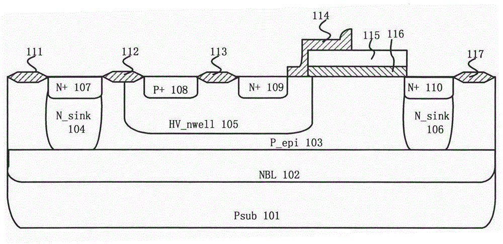
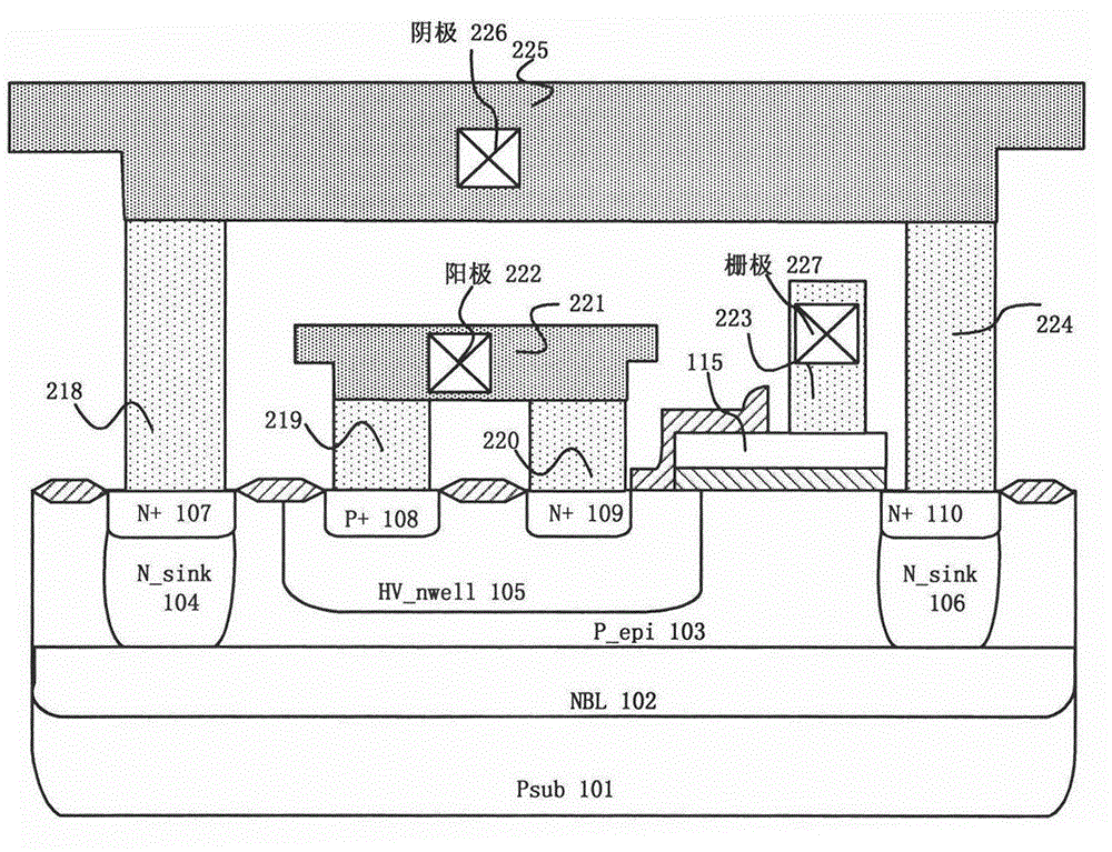
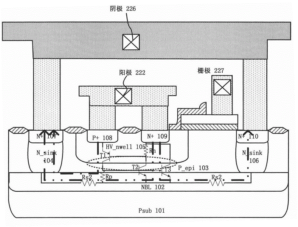
[0027] The example of the present invention designs a high-voltage ESD protection device with high sustaining voltage triggered by a vertical NPN, which not only makes full use of the characteristics of LDMOS devices with high voltage resistance and high sustaining voltage of NPN devices, but also utilizes the low on-resistance and large current leakage of SCR devices. The characteristics of discharge capability, by using N-type sinking well, N-type buried layer, P-type epitaxial layer and high-voltage deep N-well, the ESD protection device in which the reverse PN junction in the vertical NPN structure is triggered to be turned on is formed, and the device is extended The current conduction path after triggering. By elongating the length of the polysilicon gate, the withstand voltage capability and sustain voltage of the device are improved...
PUM
| Property | Measurement | Unit |
|---|---|---|
| Thickness | aaaaa | aaaaa |
Abstract
Description
Claims
Application Information