
Terahertz wave pseudo heat light source-based imaging device

An imaging device and terahertz technology, applied in the field of terahertz wave optoelectronics, can solve problems such as work stability to be further improved, high operation and maintenance costs, and limited practical development, so as to improve imaging flexibility and anti-interference capability, the effect of narrow linewidth

Inactive Publication Date: 2013-03-27
NORTHWEST UNIV
View PDF1 Cites 9 Cited by
  • Summary
  • Abstract
  • Description
  • Claims
  • Application Information

AI Technical Summary

Problems solved by technology

[0005] (1) When the terahertz wave carrying the information of the imaging object is transmitted in space, it is easy to be randomly disturbed by the external environment, such as air flow, humidity change, smoke and dust, etc., and the imaging effect will inevitably be affected, and the anti-interference ability is poor. This limits the practical application of these terahertz wave imaging technologies in harsh environments
[0006] (2) Terahertz wave radiation sources commonly used in terahertz wave imaging technology, such as pulsed terahertz wave sources based on femtosecond lasers, return wave tubes, optically pumped terahertz wave lasers, etc., are expensive, and operation and maintenance The cost is high, some are large in size, complex in operation, and the work stability needs to be further improved, which limits the development of its practicality

Method used


Image

  • Terahertz wave pseudo heat light source-based imaging device

Examples


Embodiment Construction

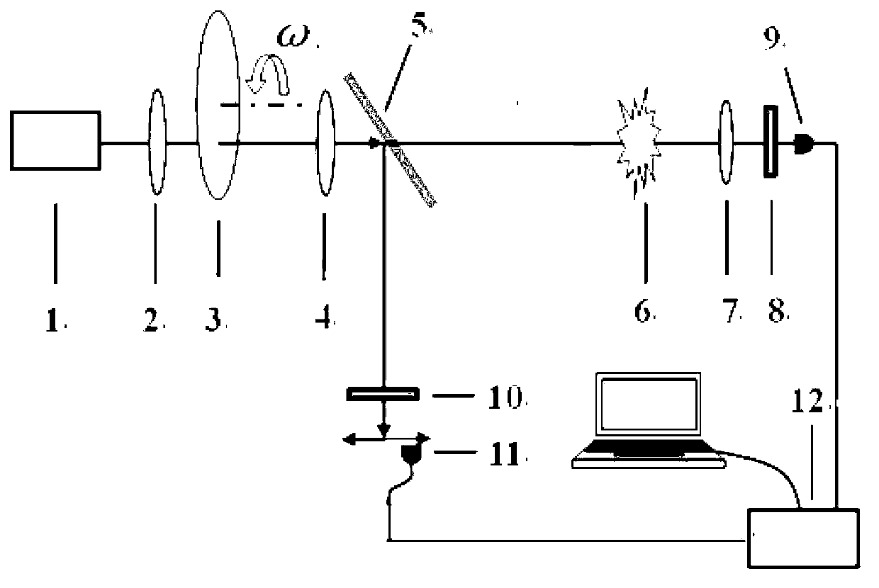
[0020] Such as figure 1 As shown, this embodiment provides an imaging device based on a terahertz wave pseudo-thermal light source, including a terahertz wave parametric oscillator 1, a terahertz wave focusing lens 2, a rotating matte silicon wafer 3, and a terahertz wave collimator A lens 4, a terahertz beam splitter 5, a terahertz transmission optical system and a terahertz reflection optical system, and a measuring device 12; wherein:

[0021] The rough silicon wafer 3 is placed near the focal point of the terahertz wave focusing lens 2, and the distance from the rough silicon wafer 3 to the terahertz wave collimating lens 4 is the focal length of the terahertz wave collimating lens 4;

[0022] The terahertz transmission optical path system is composed of an object to be imaged 6, a terahertz wave collecting lens 7, a first terahertz attenuation film 8 and a first Schottky barrier photodiode 9; wherein, the first Schottky barrier photodiode 9 Placed on the focal point of t...


PUM


Abstract

The invention discloses a terahertz wave pseudo heat light source-based imaging device. The terahertz wave pseudo heat light source-based imaging device comprises a terahertz wave parametric oscillator, a terahertz wave focusing lens, a rotating quarry-faced silicon wafer, a terahertz wave collimating lens, a terahertz wave beam splitter, a terahertz transmission light path system, a terahertz reflection light path system and a coincidence measurement circuit, wherein the terahertz transmission light path system consists of an object to be imaged, a terahertz wave collection lens, a terahertz attenuation wafer, a schottky barrier photodiode; and the terahertz reflection light path system consists of a terahertz wave attenuation wafer and a schottky barrier photodiode. The terahertz wave pseudo heat light source-based imaging device has the advantages of being simple in structure, flexible to operate, strong in anti-interference capability, and the like.

Description

technical field [0001] The invention relates to the technical field of terahertz wave optoelectronics, in particular to a terahertz wave imaging device. Background technique [0002] Terahertz waves (THz waves) refer to electromagnetic waves with frequencies in the range of 0.1-10THz (1THz=10 12 Hz), and its wave band is between millimeter wave and far infrared light in the electromagnetic spectrum. In recent years, with the rapid development of terahertz wave optoelectronic technology, terahertz wave imaging technology is changing with each passing day. At present, the most common terahertz wave imaging technology is pulsed terahertz wave time-domain spectral imaging technology. Through the Fourier transform of the terahertz wave time-domain pulse containing the imaging object information, it can obtain the spatial distribution information of its intensity and phase, and then the terahertz wave image of the object can also obtain the spatial density distribution and refra...

Claims


Application Information

Patent Timeline
IPC IPC(8): G01N21/17
Inventor 孙博
Owner NORTHWEST UNIV
Learn More