Method for manufacturing display device and etching solution composition

A technology of composition and copper alloy layer, which is applied in the direction of surface etching composition, chemical instrument and method, semiconductor/solid-state device manufacturing, etc., can solve the problem that it is difficult to fully etch the metal layer, and achieve the goal of improving productivity and simplifying the manufacturing process Effect

Active Publication Date: 2013-03-27
DONGWOO FINE CHEM CO LTD
View PDF5 Cites 10 Cited by
  • Summary
  • Abstract
  • Description
  • Claims
  • Application Information

AI Technical Summary

Problems solved by technology

In this regard, due to the different properties of the two metal layers, it is difficult to sufficiently etch these metal layers by a single etching process

Method used


Image

  • Method for manufacturing display device and etching solution composition
  • Method for manufacturing display device and etching solution composition
  • Method for manufacturing display device and etching solution composition

Examples


example 1

[0085] Based on the total weight of the mixture as 100%, 10% by weight of sodium persulfate (SPS), 1% by weight of ammonium bifluoride (ABF), 4% by weight of nitric acid (HNO 3 ), 1.5% by weight of 5-aminotetrazolium (ATZ), 1% by weight of sodium chloride (NaCl), 3% by weight of acetic acid and the balance of water are mixed together to prepare 180kg of Etching solution composition.

experiment example

[0092] (Evaluation of etching properties)

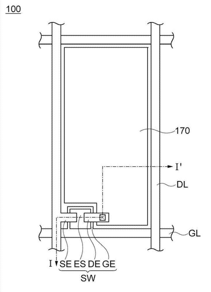
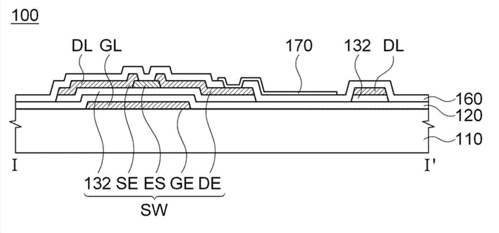
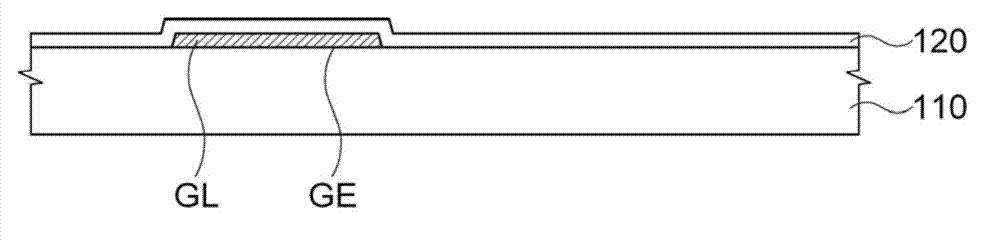
[0093] The substrate was cut into samples with a size of 550 mm × 650 mm by a diamond knife, and the substrate was manufactured by: 2 -In 2 o 3 -ZnO, HIZO) oxide semiconductor layer and a copper alloy layer containing copper and manganese, and then form a desired form of photoresist pattern on the copper alloy layer.

[0094] The prepared etching solution composition was placed in a test instrument (etcher (TFT), SEMES company) in injection etching mode and heated to a preset temperature of 30°C. Subsequently, after the temperature reaches 30°C±0.1°C, an etching process is performed. During the total etch time according to EPD (end point detector) time, an overetch of 200% is performed. Each sample is placed in the testing apparatus and the injection begins. After etching is complete, the processed sample is removed from the instrument, washed with deionized water, dried using a hot air blower, and the photoresist is removed fro...


PUM

PropertyMeasurementUnit
thicknessaaaaaaaaaa

Abstract

The invention discloses a method for manufacturing a display device and an etching solution composition which is used for the method. The etching solution composition for a copper metal layer /metal oxide layer is used to simultaneously etch a data metal layer containing the copper metal layer and an oxide semiconductor layer containing the metal oxide layer. Patterns of the data metal layer and the oxide semiconductor layer are formed in order by the etching solution composition, so as to facilitate formation of semiconductor patterns and source patterns comprising a data line, a source electrode and a drain electrode. In this way, the composition of the invention is effectively suitable for the method for manufacturing a display device, and guarantees the improvement of the production rate of thin film transistors and display devices and the reliability of the process of manufacturing the thin film transistors and the display devices.

Description

[0001] related application [0002] This application claims priority from Korean Patent Application No. 10-2011-0091917 filed with the Korean Intellectual Property Office on September 9, 2011, the entire disclosure of which is incorporated herein by reference. technical field [0003] The present invention relates to a method of manufacturing a display device using an etching solution composition for simultaneously etching a copper-based metal layer ("copper metal layer") and an oxide semiconductor layer composed of a metal oxide layer, and a method used in the method Etching solution composition for copper metal layer / metal oxide layer. Background technique [0004] A representative electronic circuit driving any semiconductor device and flat panel display device is a thin film transistor (TFT). A conventional process for manufacturing a TFT is generally provided by forming a metal thin film on a substrate as a wiring material for the gate and data, arranging a photoresis...

Claims


Application Information

Patent Timeline
Patent Type & Authority Applications(China)
IPC IPC(8): H01L21/306H01L21/3213C09K13/08C23F1/18
CPCC23F1/02C23F1/18C09K13/04G02F1/13439G02F1/1362H01L21/3213
Inventor 张尚勋尹暎晋沈庆辅
Owner DONGWOO FINE CHEM CO LTD
Why Eureka
Try Eureka