A method for enhancing the bonding strength of sog process microstructure

A technology of bonding strength and microstructure, which is applied in the direction of microstructure technology, microstructure devices, manufacturing microstructure devices, etc., can solve the problems of high requirements for bonding equipment and difficult realization, etc., so as to improve the yield of the process and reduce the Effect of Thermal Mismatch Stress, Improvement of Microstructure Bonding Strength

Inactive Publication Date: 2015-12-02
PEKING UNIV
View PDF5 Cites 0 Cited by
  • Summary
  • Abstract
  • Description
  • Claims
  • Application Information

AI Technical Summary

Problems solved by technology

However, when this method is used for anodic bonding, different stable temperatures need to be applied to the upper and lower substrates, which requires high bonding equipment and is not easy to achieve.

Method used


Image

  • A method for enhancing the bonding strength of sog process microstructure
  • A method for enhancing the bonding strength of sog process microstructure
  • A method for enhancing the bonding strength of sog process microstructure

Examples


Embodiment Construction

[0021] The present invention will be further described below through specific embodiments and accompanying drawings.

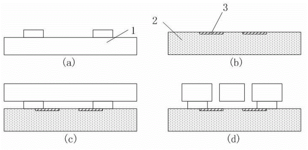
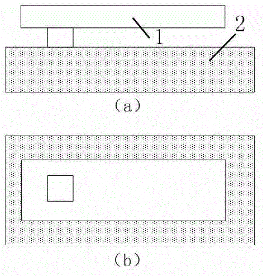
[0022] MEMS devices manufactured based on the standard process of bonding deep etch release can be roughly divided into three main parts: structure, anchor point, and substrate (glass) from top to bottom. Such as image 3 Shown are the cross-section and top views of a simple cantilever device with a single anchor, where both the structure and the anchor are made of single crystal silicon and the substrate is glass.

[0023] Due to the thermal expansion coefficient mismatch between single crystal silicon and glass materials, initial thermal stress occurs at the bottom of the anchor point after the device is fabricated, and the interface between single crystal silicon and glass, which has a certain negative impact on the reliability of the entire device structure. , when the cantilever beam is subjected to a large horizontal or vertical impact force, the corres...


PUM


Abstract

The invention discloses a method for enhancing the bonding strength of an SOG (silicon on glass) process microstructure. According to the method, an operation of microstructure bonding is implemented by using a combined anchor point structure consisting of a plurality of anchor points. Preferably, the combined anchor point is in an array form. The number of the anchor points, through which the bonding strength of the combined anchor point structure is maximal, can be determined through a stretching or shear fracture test, and taken as the number of the anchor points in the combined anchor point. The size of gaps between the anchor points in the combined anchor point can be determined according to two factors including the minimum photoetching allowed spacing and the limited spacing for keeping the facilitation of stress release. The invention also provides an MEMS (micro-electromechanical system) device using the combined anchor point structure. According to the invention, the thermal mismatch stress caused in the technological process is reduced through a reasonable design on the distribution of the anchor points, so that the bonding strength of a microstructure manufactured based on an SOG process is enhanced, therefore, the technological rate of finished products can be significantly improved, and the reliability of the MEMS device manufactured based on the SOG process can be improved.

Description

technical field [0001] The invention belongs to the field of microelectromechanical system (MEMS) device structure design, and specifically relates to a method for enhancing the bonding strength of a microstructure manufactured based on a bonding depth etch release standard process (silicon onglass, SOG), and is especially used in manufacturing based on a SOG process. The field of MEMS device structure design. Background technique [0002] Since the 1990s, microelectromechanical systems (MEMS) technology has entered a stage of rapid development, not only because of the novel concept, but also because MEMS devices have the characteristics of miniaturization, integration and better performance compared with traditional devices. Now MEMS has been widely used in automobiles, aerospace, information control, medicine, biology and other fields. [0003] Although the principles and structures of various MEMS devices are different, it is entirely possible to realize them through the...

Claims


Application Information

Patent Timeline
Patent Type & Authority Patents(China)
IPC IPC(8): B81C1/00
Inventor 何军张大成黄贤赵丹淇林琛王玮杨芳田大宇刘鹏李婷罗葵
Owner PEKING UNIV
Why Eureka
Try Eureka