Thin-film solar cell annealing device, and preparation method of copper indium gallium selenide thin-film cell absorption layer and copper zinc tin sulfide thin-film cell absorption layer

A solar cell and annealing device technology, which is applied to coatings, circuits, electrical components, etc., can solve the problems of insufficient heating capacity and low annealing efficiency of thin-film solar cell annealing devices, and achieve uniform heating, uniform selenization reaction, and good quality Effect

Inactive Publication Date: 2013-04-03
SHENZHEN INST OF ADVANCED TECH +1
View PDF14 Cites 4 Cited by
  • Summary
  • Abstract
  • Description
  • Claims
  • Application Information

AI Technical Summary

Problems solved by technology

However, because the heat needs to be transferred to the substrate through the graphite box, the heating ca...

Method used


Image

  • Thin-film solar cell annealing device, and preparation method of copper indium gallium selenide thin-film cell absorption layer and copper zinc tin sulfide thin-film cell absorption layer
  • Thin-film solar cell annealing device, and preparation method of copper indium gallium selenide thin-film cell absorption layer and copper zinc tin sulfide thin-film cell absorption layer
  • Thin-film solar cell annealing device, and preparation method of copper indium gallium selenide thin-film cell absorption layer and copper zinc tin sulfide thin-film cell absorption layer

Examples


Embodiment Construction

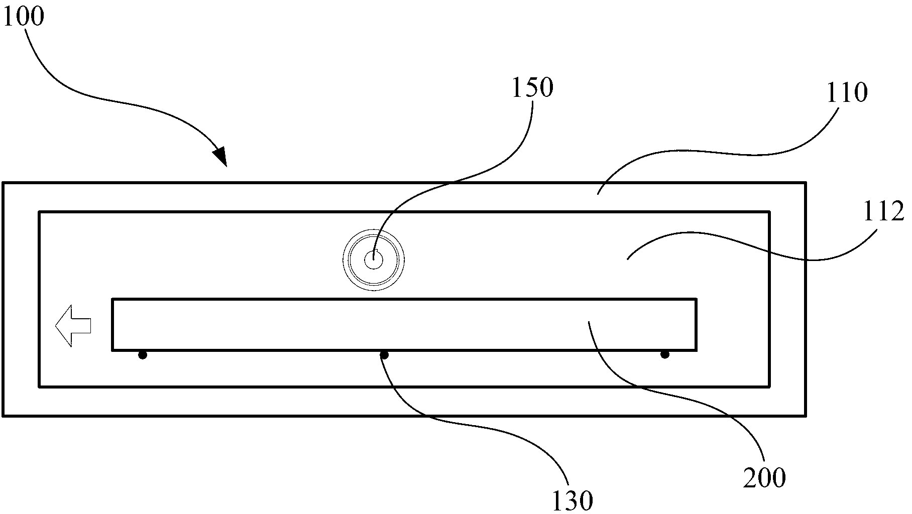
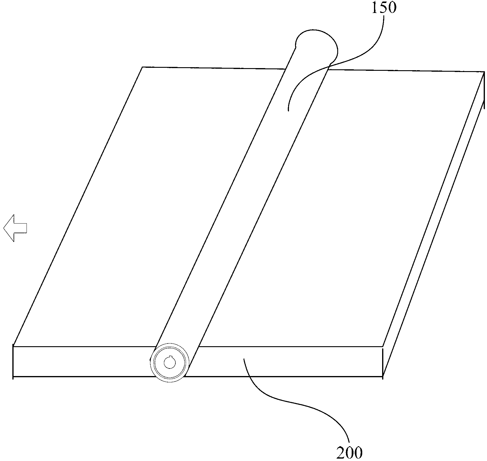
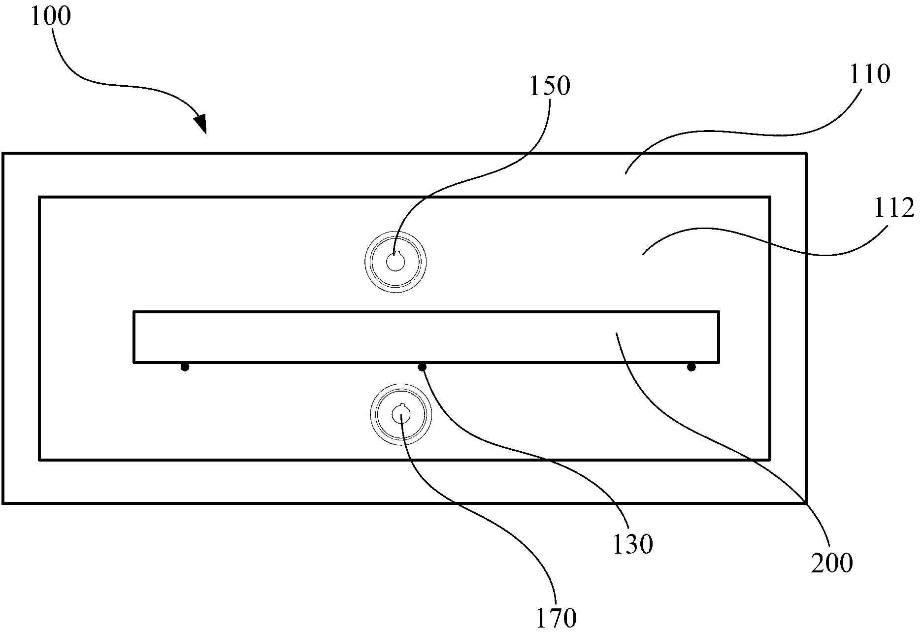
[0046] In order to facilitate the understanding of the present invention, the present invention will be described more fully below with reference to the associated drawings. Preferred embodiments of the invention are shown in the accompanying drawings. However, the present invention can be embodied in many different forms and is not limited to the embodiments described herein. On the contrary, the purpose of providing these embodiments is to make the disclosure of the present invention more thorough and comprehensive.

[0047] It should be noted that when an element is referred to as being "fixed" to another element, it can be directly on the other element or there may be an intervening element. When an element is referred to as being "connected to" another element, it can be directly connected to the other element or intervening elements may also be present. The terms "vertical," "horizontal," "left," "right," and similar expressions are used herein for purposes of illustra...


PUM


Abstract

A thin-film solar cell annealing device is used for selenizing or vulcanizing a metal film prefabrication layer on a substrate, and comprises an annealing furnace, a substrate rack and a first heating lamp tube, wherein the annealing furnace adopts a hollow structure; a sealed annealing cavity is formed inside the annealing furnace; the substrate rack is arranged on one side wall of the annealing cavity; the substrate can be loaded on the substrate rack; one end of the first heating lamp tube is arranged on one side wall of the annealing cavity; the first heating lamp tube is positioned on one side of the substrate provided with the metal film prefabrication layer; the first heating lamp tube and the substrate are arranged at an interval; a plane positioned with the first heating lamp tube and a plane positioned with the substrate rack are parallel to each other; and the first heating lamp tube and the substrate rack can conduct relative movement. In the thin-film solar cell annealing device, heat given out from the first heating lamp tube is directly radiated to the surface of the substrate, so that the fast heating capability is improved. Meanwhile, the invention further provides a preparation method of a copper indium gallium selenide thin-film cell absorption layer and a copper zinc tin sulfide thin-film cell absorption layer.

Description

technical field [0001] The invention relates to thin-film solar cell preparation technology, in particular to a thin-film solar cell annealing device, a copper indium gallium selenium thin film cell and a method for preparing an absorbing layer of a copper zinc tin sulfur thin film cell. Background technique [0002] Thin film solar cells include copper indium gallium selenide thin film batteries and copper zinc tin sulfur thin film batteries. Copper indium gallium selenide thin-film battery is a new type of green energy with both high efficiency and low cost advantages, and its photovoltaic conversion efficiency has exceeded 20% in the laboratory. Compared with existing silicon-based photovoltaic solar cells, mass production of copper indium gallium selenide thin film cells will bring greater cost advantages. [0003] Copper-zinc-tin-sulfur thin-film battery is a new energy source with great potential under research. Its advantage is that various elements required for raw ...

Claims


Application Information

Patent Timeline
IPC IPC(8): C23C14/58C23C14/06H01L31/18
CPCY02P70/521Y02P70/50
Inventor 罗海林顾光一杨春雷钟国华肖旭东
Owner SHENZHEN INST OF ADVANCED TECH
Why Eureka
Try Eureka