Wafer level packaging structure and manufacturing method thereof

A technology of wafer-level packaging and manufacturing methods, applied in semiconductor/solid-state device manufacturing, electrical components, electrical solid-state devices, etc., can solve problems such as long drilling time, increased drilling difficulty, and increased laser processing costs, and achieve improved Yield rate, effect of reducing drilling difficulty and time

Inactive Publication Date: 2013-04-03
ADVANCED SEMICON ENG INC
View PDF5 Cites 14 Cited by
  • Summary
  • Abstract
  • Description
  • Claims
  • Application Information

AI Technical Summary

Problems solved by technology

However, for packaging products that require a smaller blind hole pitch (for example, less than 100 microns) or a larger blind hole aspect ratio, the difficulty of drilling will be greatly increased
[0004] For example, for a blind hole with a small diameter to be formed on a substrate with a certain thickness, the drilling depth becomes larger due to the thickness of the substrate, making the drilling time longer, resulting in an increase in laser processing costs. The precision of the equipment also has higher requirements; subsequent blind hole plating will also greatly increase the difficulty of plating and the process time due to the larger depth of blind holes

Method used


Image

  • Wafer level packaging structure and manufacturing method thereof
  • Wafer level packaging structure and manufacturing method thereof
  • Wafer level packaging structure and manufacturing method thereof

Examples


Embodiment Construction

[0025] In order to make the above objects, features and advantages of the present invention more comprehensible, preferred embodiments of the present invention are exemplified below and described in detail in conjunction with the accompanying drawings. Furthermore, the directional terms mentioned in the present invention, such as "up", "down", "front", "back", "left", "right", "inside", "outside", "side", etc., It is only for orientation with reference to the attached drawings. Therefore, the directional terms used are used to illustrate and understand the present invention, but not to limit the present invention.

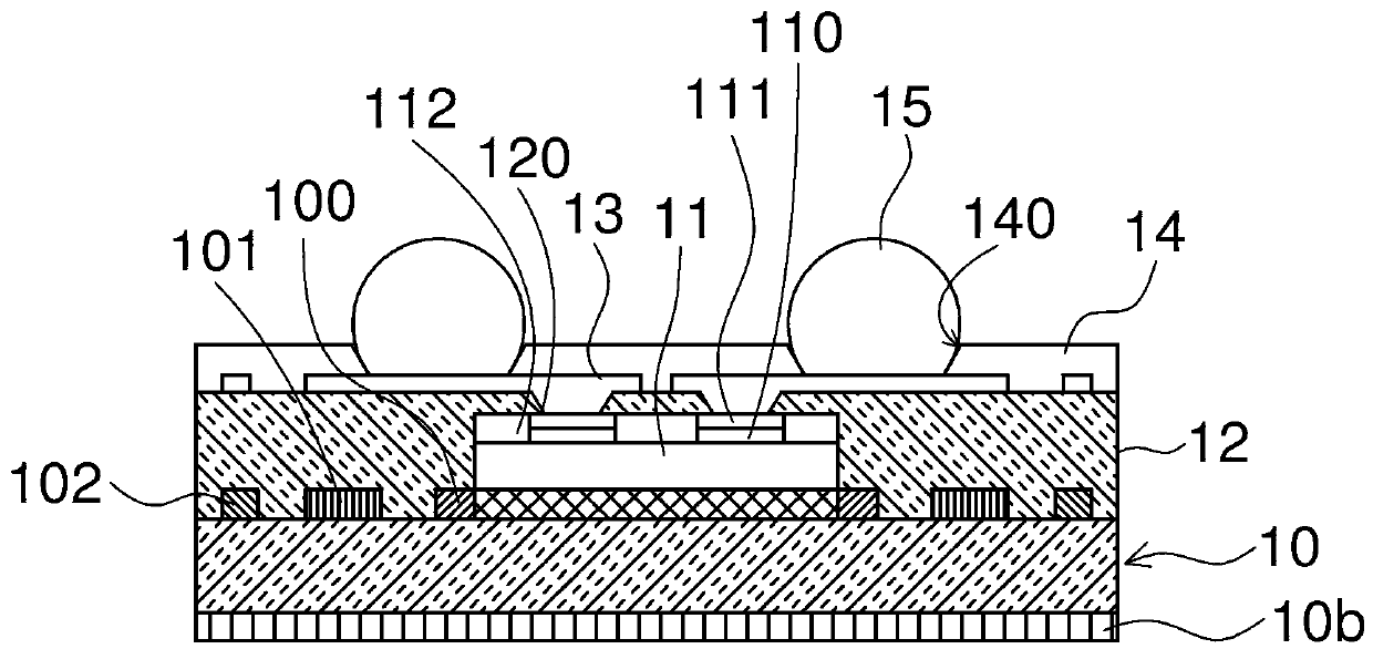
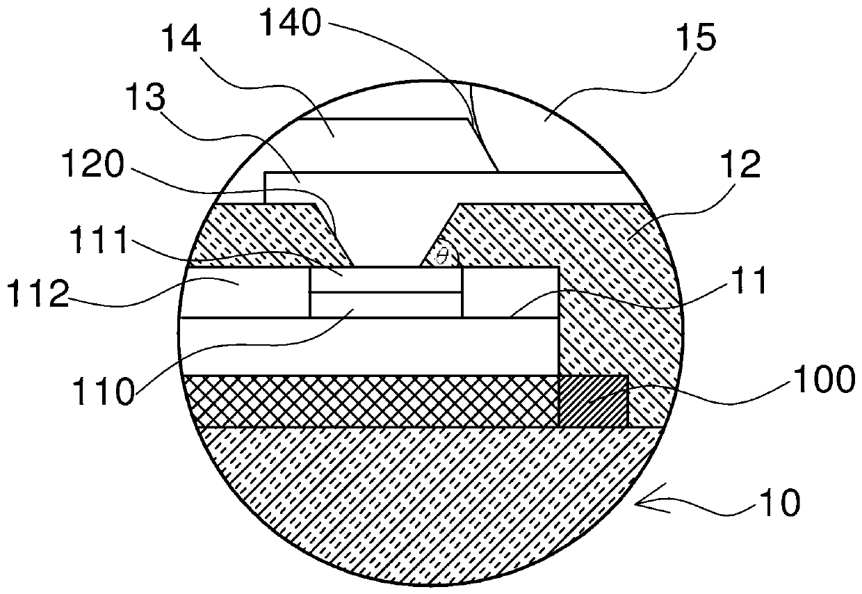
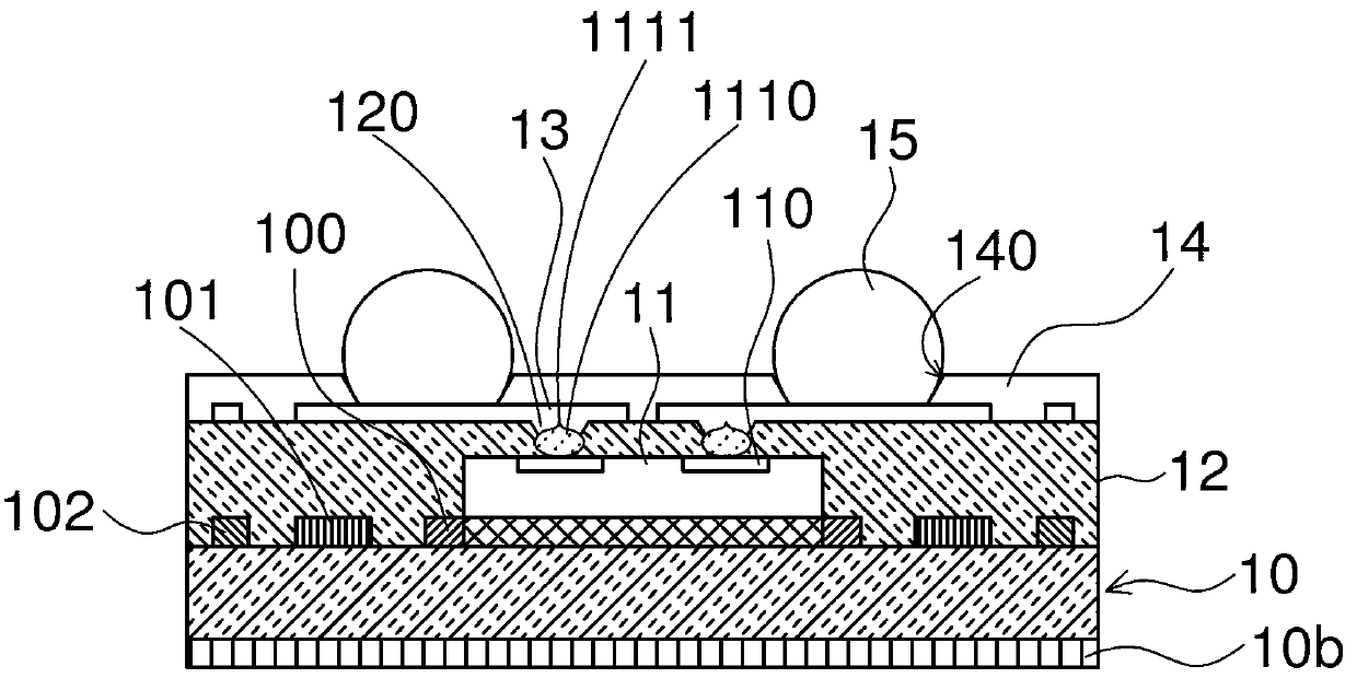
[0026] Please refer to figure 1 as shown, figure 1 is a schematic structural diagram of a wafer-level packaging structure according to an embodiment of the present invention. The wafer-level packaging structure disclosed in the present invention is a fan-out wafer-level packaging structure, including a support layer 10, a chip 11, an insulating layer 12, a rewir...


PUM


Abstract

The invention discloses a wafer level packaging structure and a manufacturing method thereof. The wafer level packaging structure comprises a supporting layer, a chip, an insulating layer and a heavy wiring layer, the chip is arranged on the supporting layer and provided with an active surface which is opposite to the supporting layer and provided with multiple welding pads, each welding pad is provided with an incrassation metal object, the insulating layer is arranged on the chip and the supporting layer and provided with multiple blind holes which respectively correspond to and expose the incrassation metal objects on the welding pads, and the heavy wiring layer is arranged on the insulating layer and electrically connected with the welding pads through the blind holes and the chip. The incrassation metal objects can relatively reduce the depth of the blind holes and lower boring difficulty on the insulating layer.

Description

technical field [0001] The invention relates to a packaging structure, in particular to a wafer-level packaging structure capable of reducing drilling reliability and a manufacturing method thereof. Background technique [0002] In today's semiconductor packaging industry, in the wafer level package (wafer level package) process, such as fan-out wafer level package (Fan-Out Wafer-Level-Package), it is often necessary to perform a through-hole manufacturing process. For example, since there is an insulating layer between the redistribution layer and the active surface of the chip, corresponding blind hole plating must be performed so that the pads of the redistribution layer and the active surface of the chip are connected through the plated blind holes in the insulating layer. form an electrical connection. [0003] The blind hole manufacturing technology adopted in the existing blind hole electroplating mainly uses laser drilling. However, for packaging products that requ...

Claims


Application Information

Patent Timeline
Patent Type & Authority Applications(China)
IPC IPC(8): H01L23/485H01L21/60
CPCH01L24/82H01L2224/04105H01L2224/12105H01L2224/19H01L2224/214H01L2224/24H01L2224/24226H01L2224/32225H01L2224/73267H01L2224/92244H01L2924/00012
Inventor 李志成
Owner ADVANCED SEMICON ENG INC
Why Eureka
Try Eureka