Preparation method and light emitting diode (LED) structure of indium gallium nitride (InGaN) base multiple quantum well structure

A multi-quantum well structure and quantum well technology, applied in electrical components, circuits, semiconductor devices, etc., can solve the problems of low luminous efficiency and low internal quantum efficiency, and achieve the effect of improving the probability of radiation recombination and increasing the internal quantum efficiency.

Active Publication Date: 2013-04-03
FOSHAN NATIONSTAR SEMICON
View PDF3 Cites 9 Cited by
  • Summary
  • Abstract
  • Description
  • Claims
  • Application Information

AI Technical Summary

Problems solved by technology

[0004] In view of this, the purpose of the present invention is to provide a method for preparing an InGaN-based multi-quantum well structure and an LED structure using the InGaN-based multi-quantum well structure, so as to overcome the low internal quantum efficiency of the multi-quantum well structure in the prior art. , The problem of low luminous efficiency of LED based on the multi-quantum well structure

Method used


Image

  • Preparation method and light emitting diode (LED) structure of indium gallium nitride (InGaN) base multiple quantum well structure
  • Preparation method and light emitting diode (LED) structure of indium gallium nitride (InGaN) base multiple quantum well structure
  • Preparation method and light emitting diode (LED) structure of indium gallium nitride (InGaN) base multiple quantum well structure

Examples


Embodiment 1

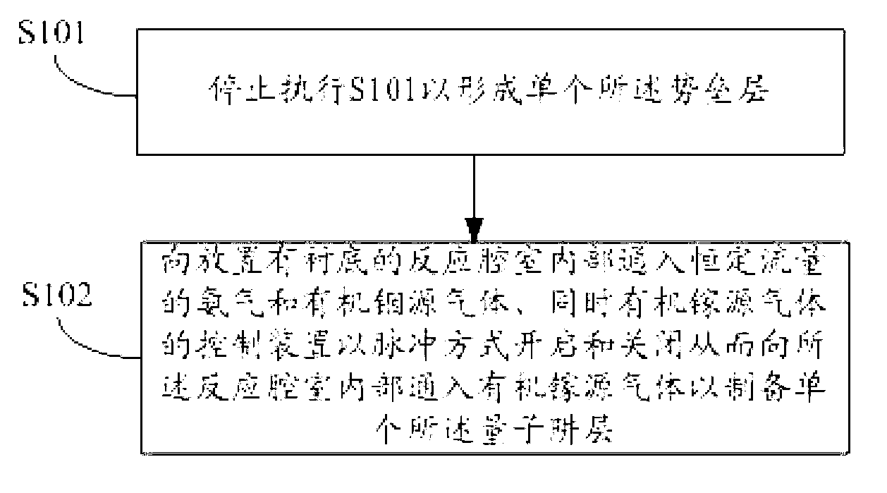
[0034] The flow chart of a certain growth cycle in the preparation method of the InGaN-based multiple quantum well structure provided by Embodiment 1 of the present invention is as follows figure 1 As shown, here "one growth cycle" (the same below) refers to the growth of a potential barrier layer and an InGaN-based quantum well layer (such as Figure 7 In the process of adjacently arranged a quantum well layer 41 and a barrier layer 42), in the actual preparation process of the InGaN-based multi-quantum well structure, it is necessary to continuously perform several growth cycles, that is, to continuously grow multiple adjacent Arranged barrier layers and InGaN-based quantum well layers can form InGaN-based multiple quantum well structures (such as Figure 7 The multiple quantum well structure in 4). For example, when the multi-quantum well structure includes alternately arranged M+1 barrier layers and M quantum well layers, M growth cycles need to be performed continuously ...

Embodiment 2

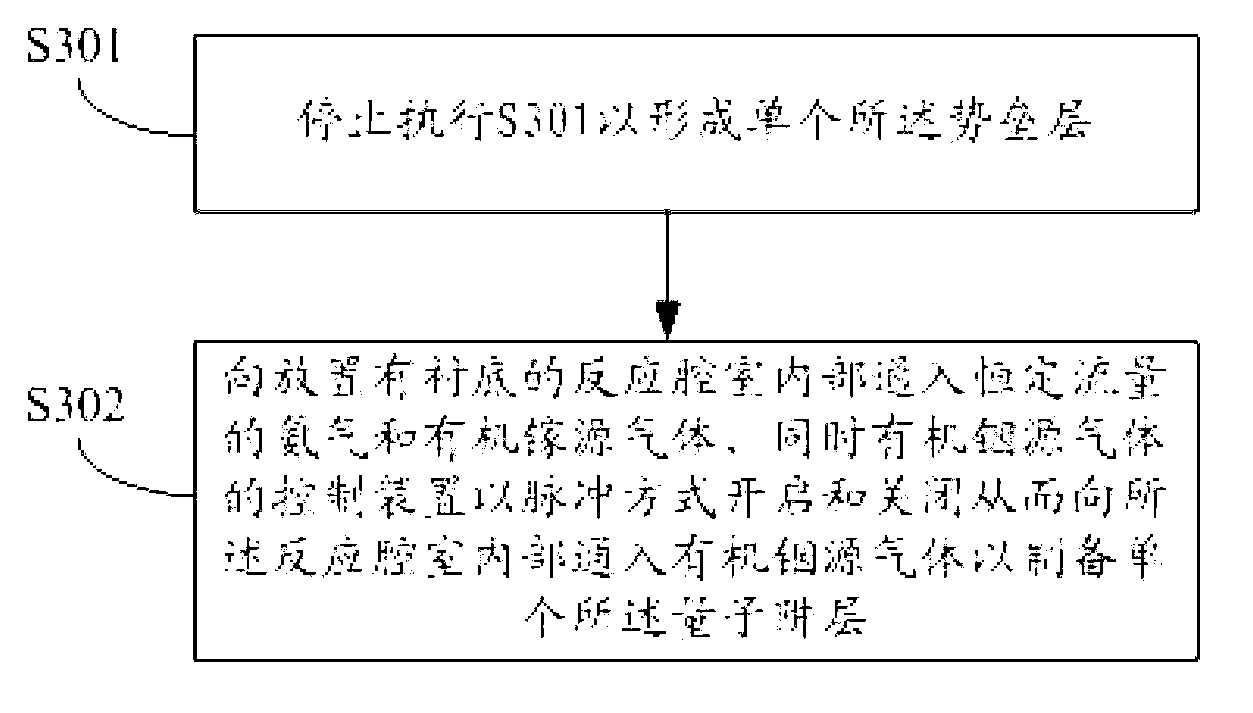
[0051] The flow chart of a certain growth cycle in the preparation method of the InGaN-based multiple quantum well structure provided by Embodiment 2 of the present invention is as follows image 3 shown.

[0052] In the second embodiment of the present invention, the following steps S301 and S302 are performed in a certain growth cycle:

[0053] Step S301: Introduce a constant flow of ammonia gas and organic gallium source gas into the reaction chamber to prepare a single barrier layer (see Figure 7 The barrier layer 42 in ), at this time, the barrier layer is GaN.

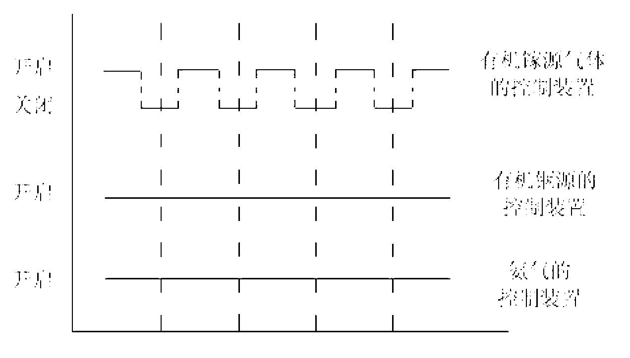
[0054] Step S302: Continuously feed organic gallium source gas and constant flow ammonia gas into the reaction chamber where the substrate is placed, and at the same time, the control device for organic indium source gas is turned on and off in a pulsed manner to vent into the organic indium source gas to prepare a single InGaN-based quantum well layer (see Figure 7 quantum well in 41).

[0055] In this ste...

Embodiment 3

[0063] The flow chart of a certain growth cycle in the preparation method of the InGaN-based multiple quantum well structure provided by Embodiment 3 of the present invention is as follows Figure 5 shown.

[0064] In the third embodiment of the present invention, the following steps S501 and S502 are performed in a certain growth cycle:

[0065] Step S501: Introduce a constant flow of ammonia gas and organic gallium source gas into the reaction chamber to prepare a single barrier layer (see Figure 7 The barrier layer 42 in ), at this time, the barrier layer is GaN.

[0066] Step S502: Continuously feed a constant flow of ammonia gas into the reaction chamber where the substrate is placed, and at the same time, the control device for the organic gallium source gas is turned on and off in a first pulse manner, so as to feed the organic gallium source gas into the reaction chamber And the control device of the organic indium source gas is turned on and off in a second pulse m...


PUM


Abstract

The invention provides a preparation method and a light emitting diode (LED) structure of an indium gallium nitride (InGaN) base multiple quantum well structure. The InGaN base multiple quantum well structure comprises a plurality of barrier layers and a plurality of quantum well layers, wherein the number of the barrier layers is M+1, and the number of the quantum well layers is M. A stage of preparing one barrier layer and one quantum well layer which are adjacent is set as a growth cycle, and the preparation method includes following steps which are performed in at least one growth cycle: step A, feeding ammonia with a constant flow rate and organic gallium source gas to the interior of a reaction chamber so as to form the single barrier layer; and step B, feeding organic indium source gas and the ammonia with the constant flow rate to the interior of a reaction chamber with a substrate placed, simultaneously opening and closing a control device of the organic gallium source gas in pulse mode, and accordingly feeding the organic gallium source gas to the interior of the reaction chamber to prepare the single quantum well layer. Luminous internal quantum efficiency of the InGaN base multiple quantum well structure can be increased by adopting the preparation method of the InGaN base multiple quantum well structure.

Description

technical field [0001] The invention belongs to the technical field of semiconductor manufacturing, and in particular relates to a preparation method of an InGaN-based multi-quantum well structure and an LED structure. Background technique [0002] GaN-based light-emitting diodes (LEDs) have the advantages of high brightness, low energy consumption, long life, and fast response. As a new type of high-efficiency solid-state light source, they are widely used in indoor lighting, landscape lighting, display screens, and signal indications. . The internal quantum efficiency of the LED structure has a decisive impact on its brightness and luminous efficiency. However, due to the bipolar input of carriers, electrons and holes are concentrated in the quantum near the N-type doped region and the P-type doped region, respectively. In the quantum wells, the carriers are unevenly distributed among the quantum wells, especially for the holes with low mobility and high effective mass, t...

Claims


Application Information

Patent Timeline
Patent Type & Authority Applications(China)
IPC IPC(8): H01L33/06H01L33/00
Inventor 李鹏张冀康学军杜雪红王垚浩
Owner FOSHAN NATIONSTAR SEMICON
Why Eureka
Try Eureka