Topological insulator structure

A technology of topological insulators and insulating substrates, applied in the direction of inorganic chemistry, non-metallic elements, Hall effect devices, etc., can solve the problems that topological insulators have not yet been manufactured, and achieve the realization of quantized anomalous Hall effect, large Effect of abnormal Hall resistance and reduction of carrier concentration

Active Publication Date: 2013-04-03
TSINGHUA UNIV +1
View PDF3 Cites 17 Cited by
  • Summary
  • Abstract
  • Description
  • Claims
  • Application Information

AI Technical Summary

Problems solved by technology

However, a topological insulator capable of quantizing the anomalous Hall effect has not actually been fabricated
Even a ferromagnetic material (including magnetically doped topological insulator )

Method used


Image

  • Topological insulator structure
  • Topological insulator structure
  • Topological insulator structure

Examples


Embodiment 1

[0070] Example 1 (T=30mK, 5QL sample, back gate control)

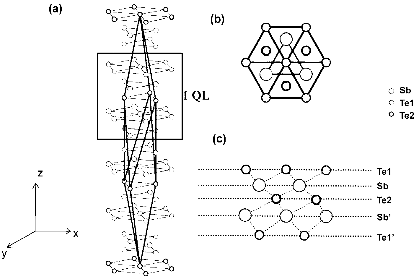
[0071] The magnetic doped topological insulator quantum well film is Cr 0.15 (Bi 0.10 Sb 0.9 ) 1.85 Te 3 , the thickness is 5QL, and the insulating substrate 30 is an STO substrate.

[0072] The Hall curves of the topological insulator structure under different back gate voltages were measured. see Figure 6-9 , at a temperature of 30 milliKelvin (mK), the R of the sample AH With the back gate voltage (V b ) changes with changes. Figure 6-9 Hysteresis also appears in the middle Hall curve, and the sample has very good ferromagnetism. When 0V≤V b ≤10V, the R of the sample AH With V b The change is small when V b at -4.5V, R AH is 25.8 kΩ. where μ 0 H in H is the magnetization, and μ 0 is the vacuum magnetic permeability, and the unit T is Tesla.

Embodiment 2

[0073] Example 2 (T=1.5K, 4QL sample, back gate control)

[0074] The magnetic doped topological insulator quantum well film is Cr 0.22 (Bi 0.22 Sb 0.78 ) 1.78 Te 3 , the thickness is 4QL, and the insulating substrate 30 is an STO substrate.

[0075] see Figure 10 , at T=1.5K, 4QL Cr on STO(111) substrate 0.22 (Bi 0.22 Sb 0.78 ) 1.78 Te 3 different V b The Hall curve under Figure 10 shown. From Figure 10 It can be seen that the Hall curve has hysteresis, and the shape of the hysteresis loop is very "square", indicating that the sample has very good ferromagnetism. by V b regulation, can obtain higher R AH . R AH With V b The increase first increases and then decreases, when V b =45V, R AH It reaches the maximum, about 10 kΩ, which is close to 0.4 quantum resistance (25.8kΩ). Figure 11 is the sample at different V b under the reluctance curve for different V b Below, the magnetoresistance curves are all "butterfly-shaped", which also shows that the ...

Embodiment 3

[0076] Example 3 (T=100mK, 4QL sample, back gate control)

[0077] The magnetic doped topological insulator quantum well film is Cr 0.22 (Bi 0.22 Sb 0.78 ) 1.78 Te 3 , the thickness is 4QL, and the insulating substrate 30 is an STO substrate.

[0078] The Hall curves of the topological insulator structure under different back gate voltages were measured. see Figure 13 , at a temperature of 100 milliKelvin (mK), the R of the sample AH With the back gate voltage (V b ) changes with changes. Figure 13 Hysteresis also appears in the middle Hall curve, and the sample has very good ferromagnetism. When 0V≤V b ≤20V, the R of the sample AH With V b little change in R AH Close to 0.6 quantum resistance (25.8kΩ). Specifically, when V b =10 V, R AH max, (R AH ) max =0.59h?e -2 , that is about 15.3kΩ. This value has far exceeded half of the quantum Hall resistance value, and is the largest abnormal Hall resistance that can be obtained in the world so far. Figur...


PUM

PropertyMeasurementUnit
thicknessaaaaaaaaaa

Abstract

The invention relates to a topological insulator structure which comprises an insulating substrate and a magnetic doped topological insulator quantum well film grown on the surface of the insulating substrate. The magnetic doped topological insulator quantum well film is made of materials shown by a chemical formula Cry (BixSb1-x) 2-yTe3, 0 (x (1, 0 (y (2, values of the x and the y are selected so that a hole carrier led in the magnetic doped topological insulator quantum well film by chromium (Cr) basically offsets an electronic carrier led in the magnetic doped topological insulator quantum well film by bismuth (Bi), and the thickness of the magnetic doped topological insulator quantum well film ranges from 3QL to 5QL (about 3nm-5nm).

Description

technical field [0001] The invention belongs to the field of condensed matter physics and relates to a topological insulator structure. Background technique [0002] The Hall effect (HE) was discovered by American physicist E. H. Hall in 1879 while studying the conductive structure of metals. When the current passes through the conductor perpendicular to the external magnetic field, a potential difference will appear between the two end faces of the conductor perpendicular to the direction of the magnetic field and current. This phenomenon is the Hall effect. Scientists subsequently discovered the anomalous Hall effect (AHE) in magnetic materials and the spin Hall effect (SHE) in semiconductors. Theoretically, the three Hall effects should exist in their corresponding quantized forms under certain conditions. In 1980, German physicist K. V. Klitzing discovered the quantum Hall effect (quantum Hall effect, QHE) (Klitzing K. V. et al., New Method for High-Accuracy Determina...

Claims


Application Information

Patent Timeline
Patent Type & Authority Applications(China)
IPC IPC(8): H01L43/06H01L43/10C01B19/00
CPCH10N52/00H10N52/01H10N50/85
Inventor 薛其坤何珂马旭村陈曦王立莉常翠祖冯硝李耀义贾金锋
Owner TSINGHUA UNIV
Why Eureka
Try Eureka