Field effect transistor of radio frequency lateral double-diffusion and preparation method thereof

A field effect transistor, lateral double diffusion technology, applied in semiconductor/solid state device manufacturing, semiconductor devices, electrical components, etc., to achieve high breakdown voltage and reduce on-resistance.

Active Publication Date: 2013-04-10
SHANGHAI HUAHONG GRACE SEMICON MFG CORP
View PDF3 Cites 9 Cited by
  • Summary
  • Abstract
  • Description
  • Claims
  • Application Information

AI Technical Summary

Problems solved by technology

However, it is still difficult to achieve a higher breakdown voltage BV (for

Method used


Image

  • Field effect transistor of radio frequency lateral double-diffusion and preparation method thereof
  • Field effect transistor of radio frequency lateral double-diffusion and preparation method thereof
  • Field effect transistor of radio frequency lateral double-diffusion and preparation method thereof

Examples


Embodiment Construction

[0056] In order to enable your examiner to have a further understanding and understanding of the purpose, features and effects of the present invention, the following detailed description with the accompanying drawings is as follows.

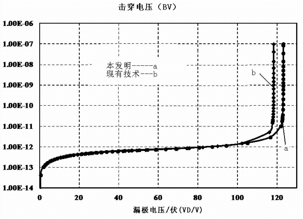
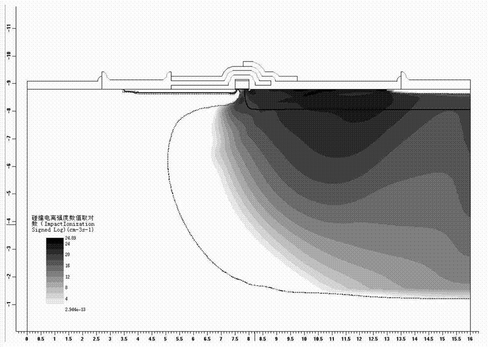
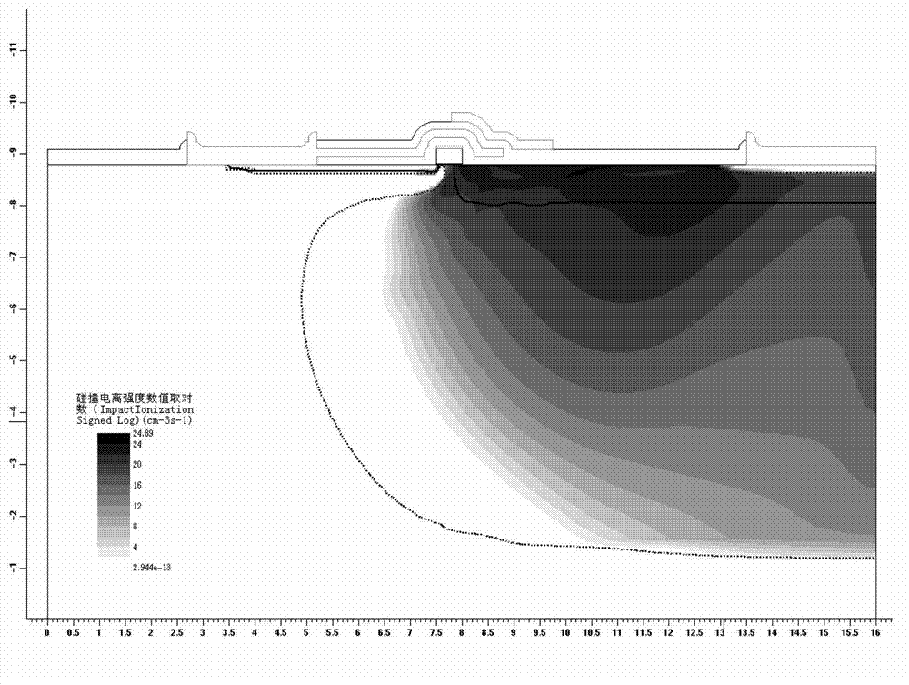
[0057] Such as figure 2 As shown, the RFLDMOS device structure of the present invention includes on the P-type substrate 21, a P-type epitaxial layer 22 is grown, and a gate oxide layer 23 is grown by thermal oxygen; polysilicon is deposited, and the photolithography plate defines and etches the polysilicon Gate 24; then on the P-type epitaxial layer 22 defined by a photolithography and ion implantation to form a lightly doped drift region (NLDD) 25; in the lightly doped drift region 25 for the second doping to form two The second NLDD implantation region 26. The two second NLDD implantation regions 26 are respectively the implantation region 261 under the first layer of Faraday Shield and the implantation region 262 under the second layer of Farad...


PUM


Abstract

The invention discloses a field effect transistor of a radio frequency lateral double-diffusion which comprises a P-type substrate. A P-type epitaxial layer is arranged on the P-type substrate, a light dope drift region is formed in the P-type epitaxial layer, and a first layer of faraday shield and a second layer of faraday shield is arranged on the upper portion of the P-type epitaxial. The light dope drift region further comprises two second time filling region of N-type light dope drift (NLDD), which respectively placed on the lower portion of the first layer of faraday shield and the second layer of faraday shield. The field effect transistor of the radio frequency lateral double-diffusion has the advantages of surpassing the performance of prior structural device, achieving higher breakdown voltage (above 120 volts), and meanwhile reducing the on-resistance of prior structural device. Meanwhile the invention further discloses a preparation method of the transistor.

Description

Technical field [0001] The invention relates to a semiconductor integrated circuit manufacturing device, in particular to a radio frequency lateral double diffused field effect transistor. The invention also relates to a manufacturing method of the transistor. Background technique [0002] The radio frequency lateral double diffused field effect transistor (RFLDMOS) device is a new generation of integrated solid-state microwave power semiconductor products that integrate semiconductor integrated circuit technology and microwave electronic technology. It has good linearity, high gain, high voltage resistance, and high output power. , Good thermal stability, high efficiency, good broadband matching performance, easy integration with MOS technology, etc., and its price is much lower than that of gallium arsenide devices. It is a very competitive power device and is widely used in GSM. PCS, power amplifiers for W-CDMA base stations, and radio broadcasting and nuclear magnetic resonan...

Claims


Application Information

Patent Timeline
IPC IPC(8): H01L29/78H01L29/06H01L21/336
CPCH01L29/404H01L29/7835H01L29/0847
Inventor 李娟娟慈朋亮钱文生韩峰胡君
Owner SHANGHAI HUAHONG GRACE SEMICON MFG CORP
Why Eureka
Try Eureka