Light emitting diode epitaxial wafer and manufacturing method thereof

A technology of light-emitting diodes and epitaxial wafers, applied in electrical components, circuits, semiconductor devices, etc., can solve problems such as quantum well band bending, lattice mismatch, etc., to reduce defect density, improve buffering and interception capabilities, and improve potential The effect of base height

Active Publication Date: 2013-04-10
HC SEMITEK CORP
View PDF4 Cites 11 Cited by
  • Summary
  • Abstract
  • Description
  • Claims
  • Application Information

AI Technical Summary

Problems solved by technology

[0005] The electron blocking layer in the existing epitaxial wafer blocks the transition of holes to the quantum well while blocking electrons, and there will be a lattice mism...

Method used


Image

  • Light emitting diode epitaxial wafer and manufacturing method thereof
  • Light emitting diode epitaxial wafer and manufacturing method thereof
  • Light emitting diode epitaxial wafer and manufacturing method thereof

Examples


Embodiment 1

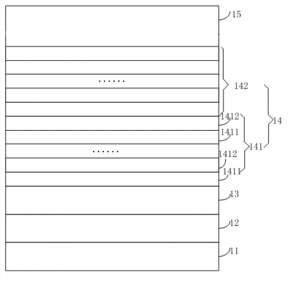
[0029] An embodiment of the present invention provides an epitaxial wafer of a light emitting diode, see figure 1 , the epitaxial wafer includes:

[0030] The substrate 11 and the buffer layer 12, n-type layer 13, multi-quantum well layer 14 and p-type layer 15 stacked in sequence on the substrate 11, the p-type layer 15 is directly arranged on the multi-quantum well layer 14, and the multi-quantum well layer 14 includes a first multi-quantum well layer 141 and a second multi-quantum well layer 142, and the first multi-quantum well layer 141 is composed of several In a Ga 1-a N quantum well layer 1411 and several quantum barrier layers 1412 are stacked alternately, and at least one of the several quantum barrier layers 1412 in the first multi-quantum well layer 141 is Al x In y Ga 1-x-y N layer, wherein, 0b Ga 1-b N quantum well layers and several quantum barrier layers are stacked alternately, and a≤b.

[0031] In a specific implementation, since the higher the temperat...

Embodiment 2

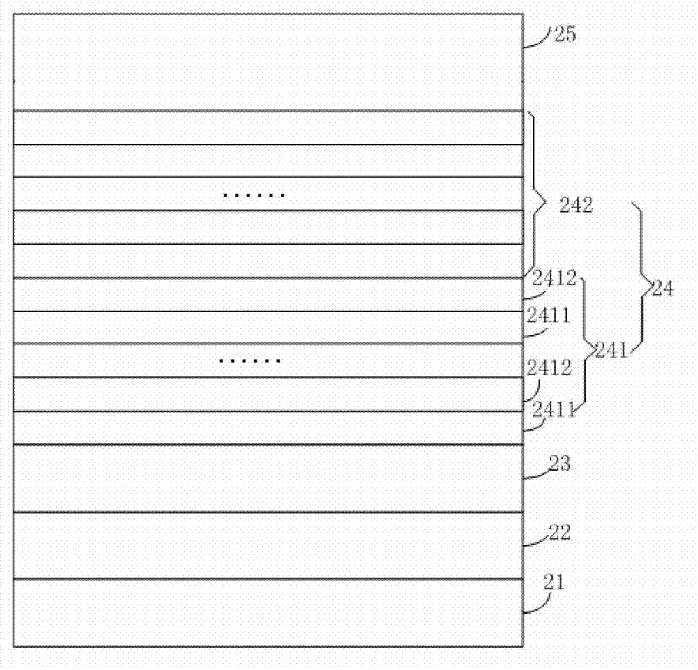
[0034] An embodiment of the present invention provides an epitaxial wafer of a light emitting diode, see figure 2 , the epitaxial wafer includes:

[0035]Substrate 21 and the buffer layer 22, n-type layer 23, multi-quantum well layer 24 and p-type layer 25 stacked in sequence on the substrate 21, the p-type layer 25 is directly arranged on the multi-quantum well layer 24, the multi-quantum well layer 24 includes a first multi-quantum well layer 241 and a second multi-quantum well layer 242, the growth temperature of the first multi-quantum well layer 241 is higher than the growth temperature of the second multi-quantum well layer 242, and the first multi-quantum well layer 141 is composed of several In a Ga 1-a N quantum well layer 2411 and several quantum barrier layers 2412 are stacked alternately, and at least one of the several quantum barrier layers 2412 in the first multi-quantum well layer 241 is Al x In y Ga 1-x-y N layer, wherein, 0b Ga 1-b N quantum well layer...

Embodiment 3

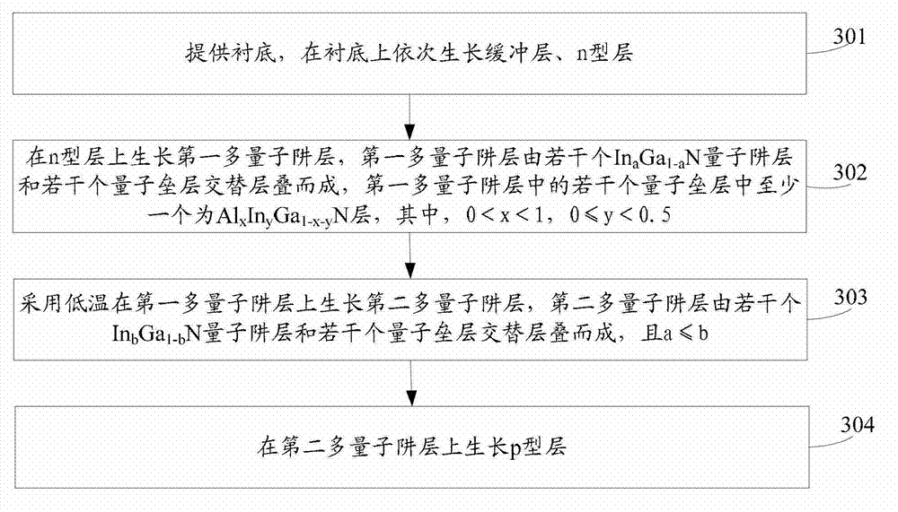
[0051] An embodiment of the present invention provides a method for manufacturing an epitaxial wafer of a light emitting diode, see image 3 , the method includes:

[0052] Step 301: providing a substrate, and sequentially growing a buffer layer and an n-type layer on the substrate.

[0053] Step 302: growing a first multi-quantum well layer on the n-type layer, the first multi-quantum well layer is composed of several In a Ga 1-a N quantum well layers and several quantum barrier layers are stacked alternately, and at least one of the several quantum barrier layers in the first multi-quantum well layer is Al x In y Ga 1-x-y N layers, where 0

[0054] Step 303: Using low temperature to grow a second multi-quantum well layer on the first multi-quantum well layer, the second multi-quantum well layer is composed of several In b Ga 1-b N quantum well layers and several quantum barrier layers are stacked alternately, and a≤b.

[0055] In a specific implementati...


PUM

PropertyMeasurementUnit
Thicknessaaaaaaaaaa
Thicknessaaaaaaaaaa
Thicknessaaaaaaaaaa

Abstract

The invention discloses a light emitting diode epitaxial wafer and a manufacturing method of the light emitting diode epitaxial wafer and belongs to the technical field of semiconductors. The epitaxial wafer comprises a substrate, a buffer layer, an n-type layer, a multi-quantum well layer and a p-type layer, the buffer layer, the n-type layer, the multi-quantum well layer and the p-type layer are stacked on the substrate in sequence, the p-type layer is directly arranged on the multi-quantum well layer which comprises a first multi-quantum well layer and a second multi-quantum well layer, a plurality of InaGa1-aN quantum well layers and a plurality of quantum barrier layers are stacked alternately to form the first multi-quantum well layer, at least one of the quantum barrier layers is the AlxInyGa1-x-yN layer, wherein 0 <x <1, 0<= y <0.5. A plurality of InbGa1-bN quantum well layers and a plurality of quantum barrier layers are stacked alternately to form the second multi-quantum well layer, and a <=b. Due to the scheme, the defect concentration of the second multi-quantum well layer is reduced, barrier height is increased, buffering and intercepting abilities are improved, luminous efficiency of devices is increased, and the problems of lattice mismatch and band bending caused by an electron blocking layer are solved.

Description

technical field [0001] The invention relates to the technical field of semiconductors, in particular to an epitaxial wafer of a light emitting diode and a manufacturing method thereof. Background technique [0002] The light-emitting diode chip is a semiconductor crystal, which is the core component of the light-emitting diode. A light emitting diode chip includes an epitaxial wafer and electrodes fabricated on the epitaxial wafer. [0003] Among them, the epitaxial wafer includes a substrate and a buffer layer, an n-type layer, a multi-quantum well layer and a p-type layer stacked on the substrate in sequence, and the multi-quantum well layer is a multilayer formed by the alternate growth of quantum barrier layers and quantum well layers. structure, and the quantum barrier layer and the quantum well layer are made of different materials. The quantum barrier layer in the existing multi-quantum well layer is generally made of undoped GaN, and the quantum well layer is genera...

Claims


Application Information

Patent Timeline
IPC IPC(8): H01L33/06H01L33/02
Inventor 王明军魏世祯胡加辉
Owner HC SEMITEK CORP
Why Eureka
Try Eureka