Surface plasmon electro excitation source and manufacturing method thereof
A surface plasmon and electro-excitation technology, applied in circuits, electrical components, semiconductor devices, etc., can solve problems such as low internal quantum efficiency, incompatibility between organic light-emitting dielectric materials and process integrated circuit technology, and small light-emitting wavelength range. Problems, to achieve high internal quantum efficiency, large luminous wavelength range, and easy integration
- Summary
- Abstract
- Description
- Claims
- Application Information
AI Technical Summary
Problems solved by technology
Method used
Image

Examples
Embodiment 1
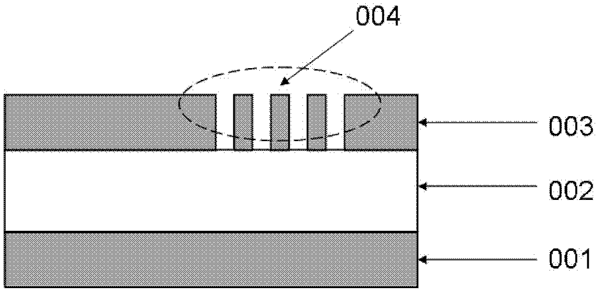
[0047] The invention provides a surface plasmon electric excitation source, its structure is as follows figure 1 shown, including:
[0048] The first metal layer 001 has a thickness of about 100nm and is made of silver;
[0049] The second metal layer 003 has a thickness of about 100nm and is made of silver;
[0050] The quantum well layer 002 between the first metal layer 001 and the second metal layer 003 is made of Al 0.3 Ga 0.7 As / GaAs / Al 0.3 Ga 0.7 Composed of As, the thickness of the AlGaAs layer is 40nm, and the thickness of the GaAs layer is 30nm;
[0051] The outcoupling structure 004 in the second metal layer 003 is a bar grating with a period of 300 nm, a duty ratio of 1:1, and a total width of the grating area of 3 microns.
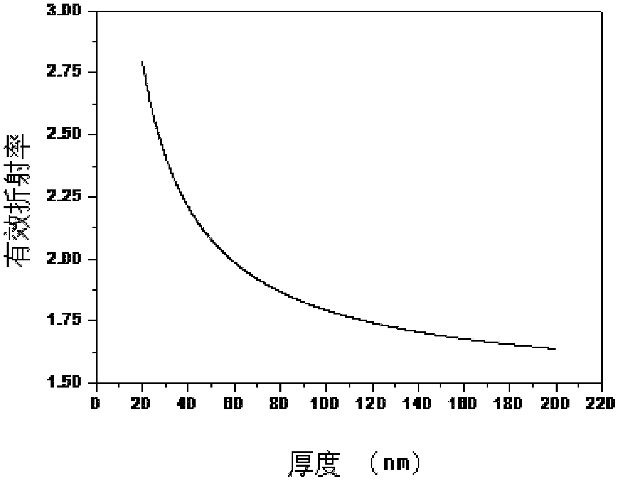
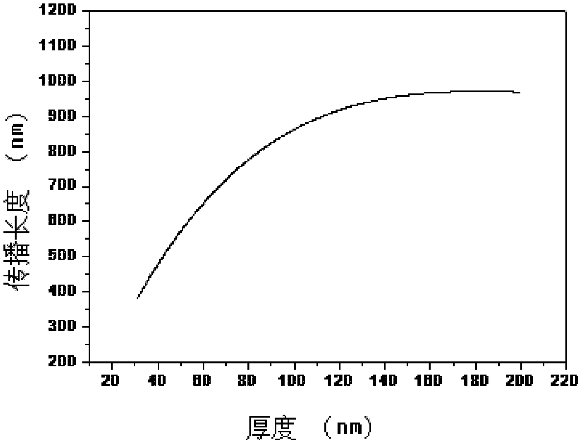
[0052] According to the surface plasmon electric excitation source provided in this embodiment, in the quantum well layer structure AlGaAs / GaAs / AlGaAs, the ratio of Al and Ga in the AlGaAs layer can be changed in the range of 0.2:0.8-0...
Embodiment 2
[0058] This embodiment provides a surface plasmon electric excitation source, the structure of which is as follows Figure 4 shown, including:
[0059] Silicon substrate 110;
[0060] The bonding metal layer 111 on the silicon substrate 110 has a thickness of about 100 nm, and the bonding metal layer 111 is made of Au;
[0061] The first metal layer 107 on the bonding metal layer 111 is made of Au with a thickness of about 100 nm;
[0062] The p-type ohmic contact layer 106 on the first metal layer 107 is made of GaAs with a doping concentration of about 10 15 cm -3 , with a thickness of 25nm;
[0063] The quantum well layer 105 on the p-type ohmic contact layer 106 is made of Al 0.3 Ga 0.7 As / GaAs / Al 0.3 Ga 0.7 Composed of As, the thickness of the AlGaAs layer is 25nm, and the thickness of the GaAs layer is 15nm;
[0064] The n-type ohmic contact layer 104 on the quantum well layer 105 is made of GaAs with a doping concentration of about 10 17 cm -3 , with a thickn...
Embodiment 3
[0075] According to an embodiment of the present invention, a method for manufacturing a surface plasmon electric excitation source is also provided, the process flow of which is as follows Image 6 (a) to Image 6 (f), including:
[0076] a) Grow a 25nm GaAs buffer layer 102, a 100nm GaInP etch barrier layer 103, and an n-type GaAs ohmic contact layer 104 (thickness 25nm, doping concentration 10nm) on the GaAs substrate 101 by MOCVD 17 cm -3 ), Al 0.3 Ga 0.7 As / GaAs / Al 0.3 Ga 0.7 As quantum well layer 105 (AlGaAs layer thickness is 25nm, GaAs layer thickness is 15nm), p-type GaAs ohmic contact layer 106 (thickness is 25nm, doping concentration is 10nm 15 cm -3 ), forming a quantum well epitaxial wafer;
[0077] b) On the p-type GaAs ohmic contact layer 106 of the silicon substrate 110 and the quantum well epitaxial wafer, the electron beam deposits the bonding metal layer 111 and the first metal layer 107 respectively, and the thickness of the bonding metal layer 111 ...
PUM
| Property | Measurement | Unit |
|---|---|---|
| Doping concentration | aaaaa | aaaaa |
| Doping concentration | aaaaa | aaaaa |
| Thickness | aaaaa | aaaaa |
Abstract
Description
Claims
Application Information