
Epitaxial structure of LED (Light Emitting Diode)

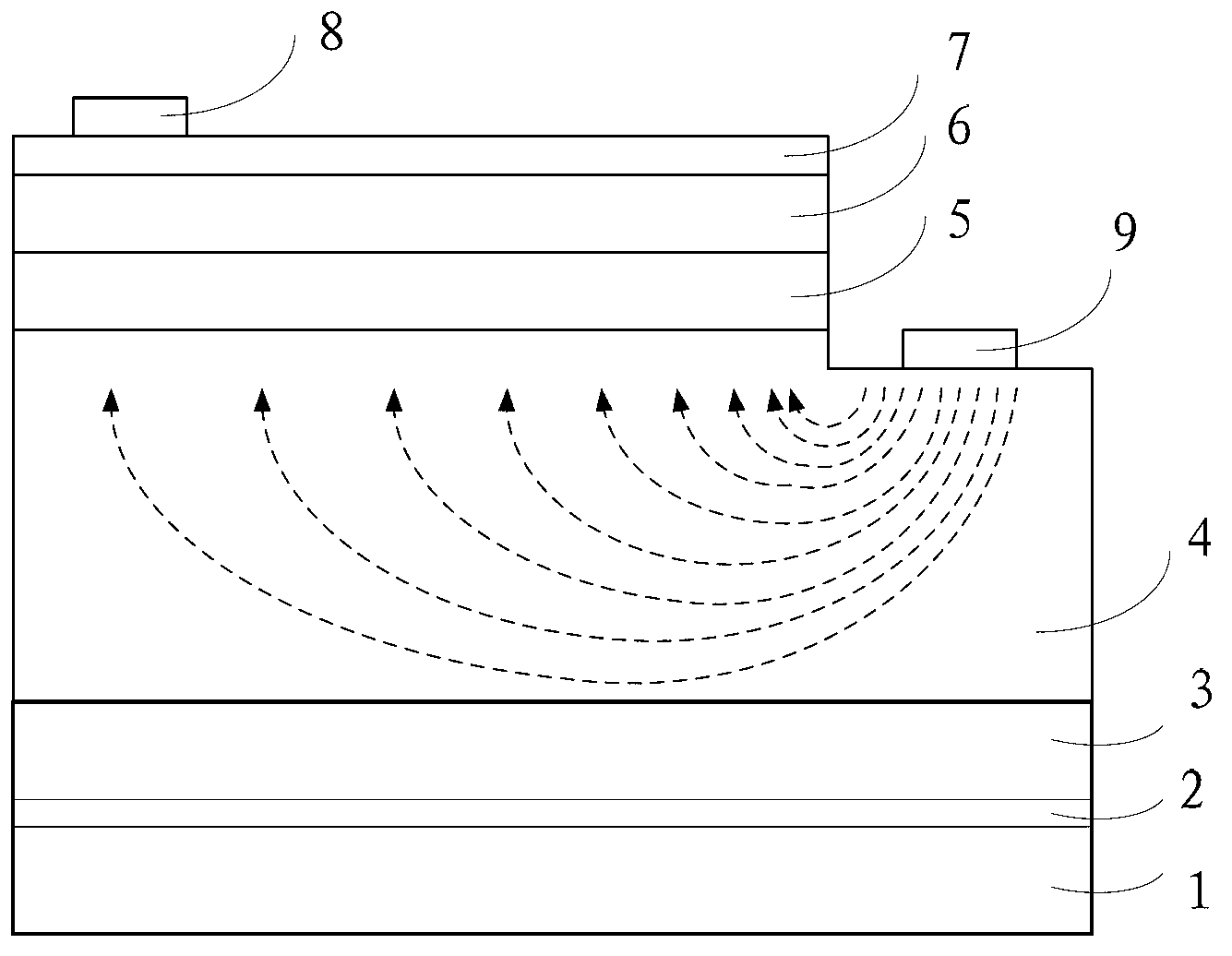
An epitaxial structure, p-type technology, applied in the direction of electrical components, circuits, semiconductor devices, etc., can solve the problem of uneven distribution of current density, achieve the effects of improving luminous efficiency and reliability, convenient manufacture, and simple structure

Inactive Publication Date: 2013-05-01
AQUALITE CO LTD
View PDF6 Cites 4 Cited by
  • Summary
  • Abstract
  • Description
  • Claims
  • Application Information

AI Technical Summary

Problems solved by technology

[0004] The technical problem to be solved by the present invention is to provide an LED epitaxial structure that can effectively solve the problem of uneven distribution of LED current density and greatly improve LED luminous efficiency.

Method used


Image

  • Epitaxial structure of LED (Light Emitting Diode)
  • Epitaxial structure of LED (Light Emitting Diode)
  • Epitaxial structure of LED (Light Emitting Diode)

Examples


Embodiment Construction

[0017] The principles and features of the present invention are described below in conjunction with the accompanying drawings, and the examples given are only used to explain the present invention, and are not intended to limit the scope of the present invention.

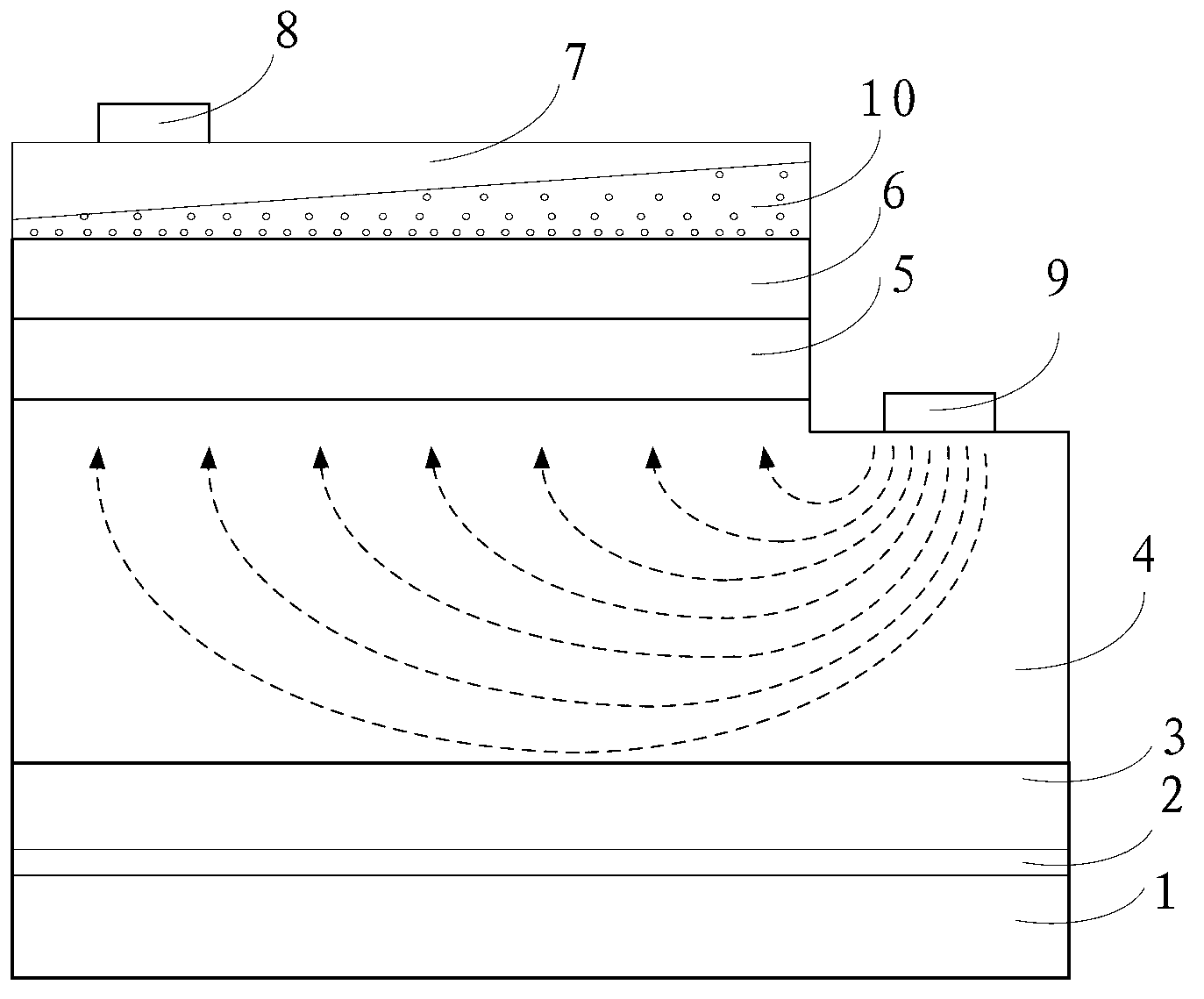
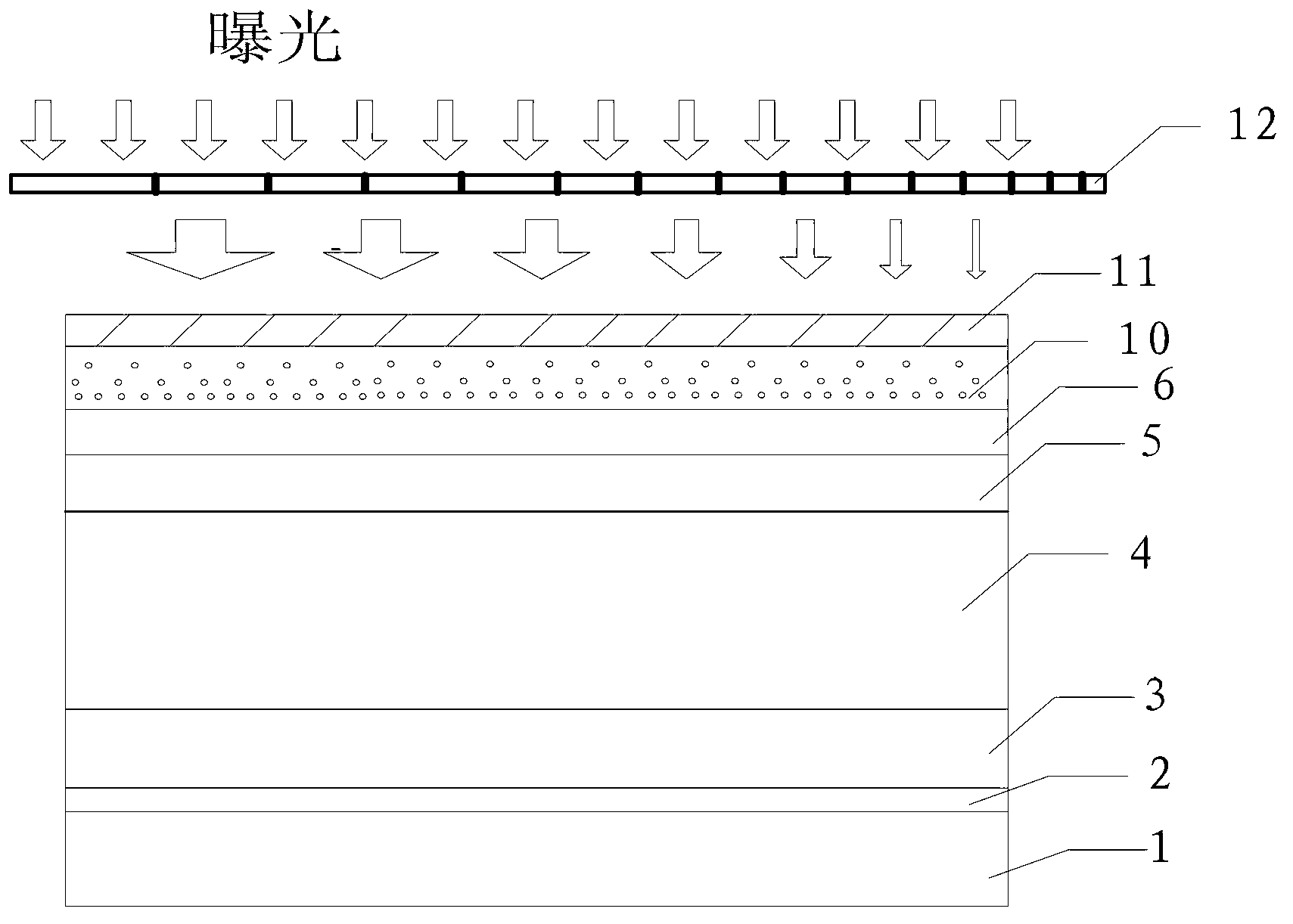
[0018] Such as figure 2 As shown, an LED epitaxial structure includes a substrate 1, a transition layer 2, a u-type gallium nitride layer 3, an n-type gallium nitride layer 4, a multi-quantum well layer 5, and a p-type gallium nitride layer 6 stacked in sequence. , ITO tin-doped indium oxide layer 7, p-type electrode 8 and n-type electrode 9 formed on the n-type gallium nitride layer, also includes a p-type contact layer 10, the p-type contact layer 10 is between p-type nitride Between the gallium layer 6 and the ITO tin-doped indium oxide layer 7, there is a wedge-shaped structure, and the hole concentration of the p-type contact layer 10 gradually changes, and the hole concentration near the p-type gallium nitrid...


PUM

PropertyMeasurementUnit
thicknessaaaaaaaaaa

Abstract

The invention relates to an epitaxial structure of an LED (Light Emitting Diode). The epitaxial structure comprises a substrate, a transition layer, a u-shaped gallium nitride layer, an n-shaped gallium nitride layer, a multiple-quantum-well layer, a p-shaped gallium nitride layer, an ITO (Indium Tin Oxide)-doped layer, a p-shaped electrode, an n-shaped electrode and a p-shaped contact layer, wherein the substrate, the transition layer, the u-shaped gallium nitride layer, the n-shaped gallium nitride layer, the multiple-quantum-well layer, the p-shaped gallium nitride layer, the ITO tin-doped indium oxide layer and the p-shaped electrode are sequentially overlapped, the n-shaped electrode is formed on the n-shaped gallium nitride layer, the p-shaped contact layer is located between the p-shaped gallium nitride layer and the ITO-doped layer and is of a wedge-shaped structure, the hole concentration of the p-shaped contact layer changes gradually, the hole concentration of one side of the p-shaped contact layer, close to the p-shaped gallium nitride layer, is high, and the hole concentration of one side of the p-shaped contact layer, away from the p-shaped gallium nitride layer, is low. The epitaxial structure of the LED, provided by the invention, has the advantages of simple structure, convenience in manufacture, and the like; and compared with the traditional structure, the efficiency and reliability of light emitting of the LED can be greatly improved.

Description

technical field [0001] The invention relates to the technical field of semiconductors, in particular to an LED epitaxial structure. Background technique [0002] In recent years, Group III nitride semiconductor materials (AlN, GaN, and InN) have been widely used in microelectronics such as solid-state lighting, solid-state lasers, optical information storage, and ultraviolet detectors due to their wide direct bandgap, good thermal and chemical stability, etc. And optoelectronic devices have significant advantages, and have made breakthroughs in research and application in recent years, especially in the context of energy supply and environmental pollution issues, semiconductor lighting sources as a high-efficiency, energy-saving, Devices with outstanding characteristics such as environmental protection, long life, and easy maintenance have attracted the attention of the world. [0003] The growth of epitaxial structures is the key technology of LED chips, and how to improve...

Claims


Application Information

Patent Timeline
Patent Type & Authority Applications(China)
IPC IPC(8): H01L33/02H01L33/14
Inventor 李鸿建靳彩霞董志江
Owner AQUALITE CO LTD
Learn More