An Electric Field-Induced Fabrication Process of Two-Level Structures for Dry Adhesion

A technology of electric field induction and preparation technology, which is applied in the direction of technology for producing decorative surface effects, microstructure technology, microstructure devices, etc., can solve the problems of limited application, complicated process, poor material adaptability, etc., to improve processing efficiency, The process route is simple and the effect of reducing manufacturing cost

Active Publication Date: 2015-08-26
XI AN JIAOTONG UNIV
View PDF7 Cites 0 Cited by
  • Summary
  • Abstract
  • Description
  • Claims
  • Application Information

AI Technical Summary

Problems solved by technology

However, the traditional preparation method has many shortcomings in terms of large-area preparation and forming efficiency: (1) The process is complicated, such as AFM etching method, which needs to use AFM to carve holes point by point on the paraffin surface, then inject liquid materials, and after cooling Removal of paraffin; (2) Precise equipment, such as plasma etching and photolithography technology, requires expensive and complex processing equipment; (3) Process parameters need to be precisely controlled, such as the formation of holes in alumina templates, which requires changing the voltage and solution acidity. The control of the pore size and pores of alumina pores; (4) Poor material adaptability, such as the preparation method of arrayed carbon nanotubes, requires the use of CVD (chemical vapor deposition) to realize the preparation of carbon nanotubes, but the high temperature environment in the CVD process is limited The application of some polymers and other materials

Method used


Image

  • An Electric Field-Induced Fabrication Process of Two-Level Structures for Dry Adhesion
  • An Electric Field-Induced Fabrication Process of Two-Level Structures for Dry Adhesion
  • An Electric Field-Induced Fabrication Process of Two-Level Structures for Dry Adhesion

Examples


Embodiment Construction

[0018] The present invention will be described in detail below in conjunction with the accompanying drawings.

[0019] An electric field-induced preparation process for a two-stage structure for dry adhesion, comprising the following steps:

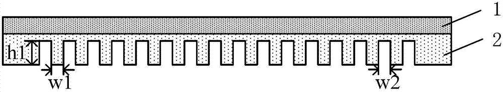
[0020] The first step is the preparation of the induced template: a pattern structure template of the second-level structure in the two-level structure is prepared on the surface of the Si wafer by photolithography, and a layer of micro-nano structure of PDMS or fluororesin 2, to obtain transparent inducible templates, such as figure 1 shown;

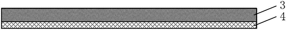
[0021] The second step, the selection and processing of the base material: use FTO or ITO glass 4 as the base material, and use a glue leveler to spin coat a layer of UV photocurable polymer material 3 on its surface. The thickness of the UV photocurable polymer material is micron scale, such as figure 2 as shown,

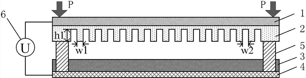
[0022] The third step, the electric field induces polymer rheological shaping:...


PUM


Abstract

The invention provides an induction preparation process for an electric field with a dry adhesion type two-level structure. The induction preparation process comprises the following steps of: at first, preparing an induction template; secondly, selecting and processing a base material; thirdly, curing a polymer material by using UV (Ultra Violet) light through induction of the electric field for rheological forming; and finally, curing and de-molding the polymer material cured by the UV light, so as to obtain a crystal structure, namely a micro-micro or micro-nanometer two-level structure. The process provided by the invention can be widely applied to aspects of a conveyor belt, a mechanical arm, a micro-sucker and the like.

Description

technical field [0001] The invention belongs to the field of dry-adhesive two-stage structure in micro-nano manufacturing, and in particular relates to an electric field-induced preparation process for dry-adhesive two-stage structure. Background technique [0002] Kellar Autumn and others in the United States studied gecko feet and found that the two-level structure on its surface has a strong adsorption capacity, which can effectively enhance the friction on the surface of objects, and can be widely used in belt conveyors, manipulators, micro-suction cups, etc. At present, the conventional two-level structure preparation methods mainly include: AFM (atomic force) etching method, hole injection molding using alumina template, plasma etching method, photolithography technology and array carbon nanotube preparation and other methods. However, the traditional preparation method has many shortcomings in terms of large-area preparation and forming efficiency: (1) The process is ...

Claims


Application Information

Patent Timeline
Patent Type & Authority Patents(China)
IPC IPC(8): B81C1/00
Inventor 邵金友丁玉成田洪淼李祥明胡鸿姜承宝
Owner XI AN JIAOTONG UNIV
Why Eureka
Try Eureka