
X-ray detector

A technology of ray detection and detection device, which is applied in the field of X-ray detection optical devices, can solve the problems of difficult detection, unclear image, large noise, etc., and achieve the effect of simple structure and clear imaging

Inactive Publication Date: 2013-05-29
XIAN ZHONGKEMAITE ELECTRONICS TECH EQUIP
View PDF0 Cites 4 Cited by
  • Summary
  • Abstract
  • Description
  • Claims
  • Application Information

AI Technical Summary

Problems solved by technology

[0003] AXI (Automatic X-ray Inspection) detection technology has begun to rise, and it is mostly used for non-destructive testing of circuit boards. When the assembled circuit board enters the machine along the guide rail, the X-ray emission tube located above the circuit board emits X-rays. After passing through the circuit board, it is received by the detector placed below. Since the solder joint contains lead that can absorb a large amount of X-rays, compared with the X-rays that pass through glass fiber, copper, silicon and other materials, the radiation on the solder joint The X-rays on the surface are absorbed in a large amount, and a good image is produced in the form of black spots, which makes the analysis of solder joints quite intuitive, so a simple image analysis algorithm can automatically and reliably inspect solder joint defects, which early X-ray inspections could not Meet the requirements of real-time imaging and real-time detection, and the image formed by the imaging system is not clear, the noise is large, etc., which makes the detection difficult

Method used


Image

  • X-ray detector

Examples


Embodiment Construction

[0013] The present invention will be described in further detail below.

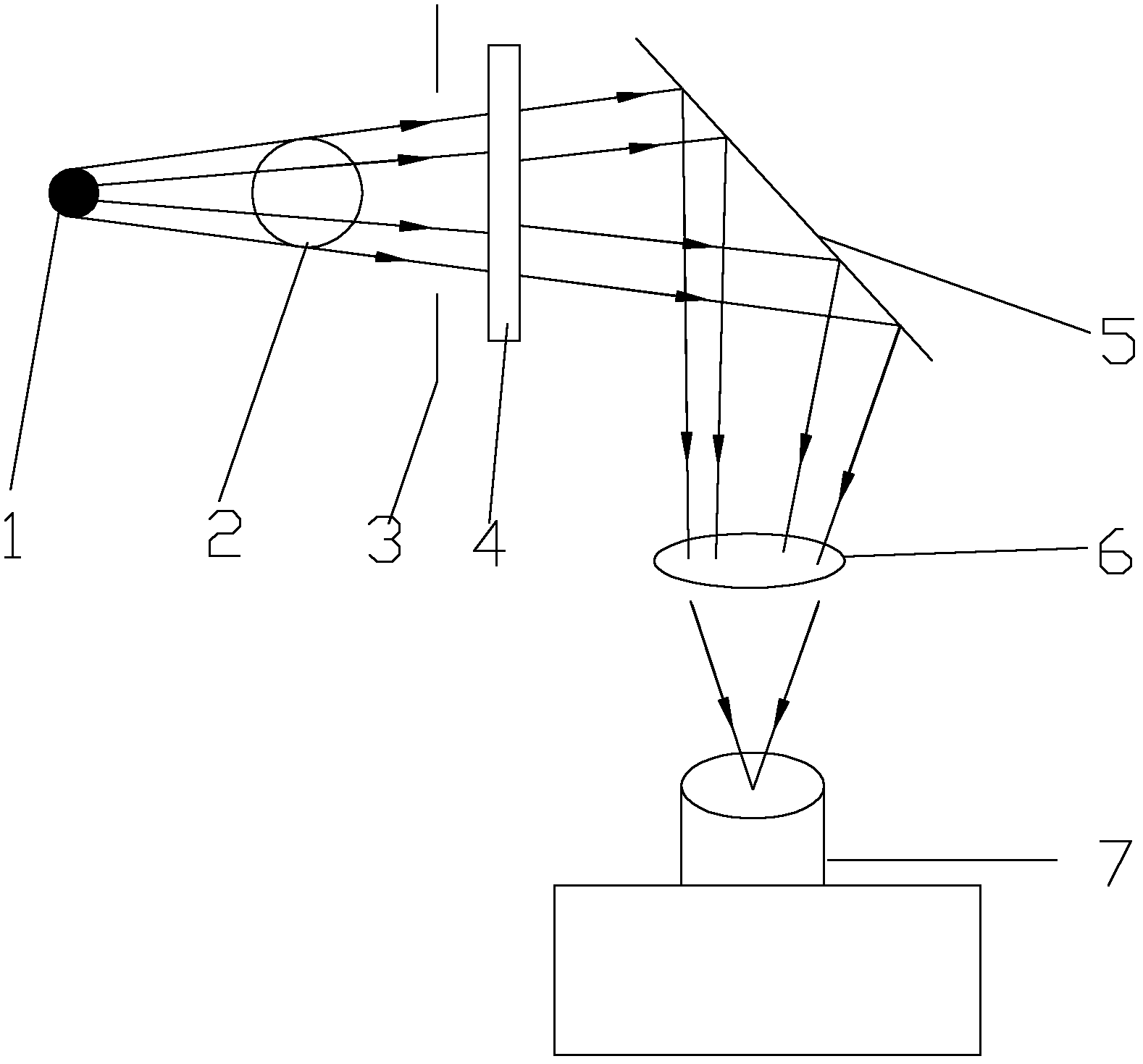
[0014] With reference to accompanying drawing, X-ray detecting device is made up of x-ray source 1, visible light conversion screen 4, aperture 3, plane mirror 5, convex lens 6 and CCD image sensor 7, is characterized in that, x-ray source 1, aperture 3 and the visible light conversion screen 4 are sequentially arranged directly in front of the plane mirror 5, and the bottom of the plane mirror 5 is sequentially provided with a convex lens 6 and a CCD image sensor 7;

[0015] A measured object 2 is arranged between the x-ray source 1 and the diaphragm 3;

[0016] The aperture 3 can remove stray light in the device;

[0017] The surface of the plane mirror 5 is coated with a high reflection film;

[0018] When the x-rays pass through the measured object 2, use the aperture 3 to remove stray light in the device, and when the x-rays pass through the visible light conversion screen 4, the x-ray image can b...


PUM


Abstract

An X-ray detector comprises an X-ray source, a visible light conversion screen, a diaphragm, a plane mirror, a convex lens and a CCD (charge coupled device) image sensor. The X-ray source, the diaphragm and the visible light conversion screen are disposed right in front of the plane mirror sequentially. The convex lens and the CCD image sensor are disposed below the plane mirror sequentially. X-ray images are directly converted into visible light images by the visible light conversion screen, the visible light is then diverted and converged by the plane mirror and a lens system, and the CCD image sensor acquires the images and converts light signals into electrical signals.

Description

technical field [0001] The invention provides an optical detection system, in particular to an X-ray detection optical device, which utilizes X-rays to form an optical imaging system through a visible light conversion screen and reflectors to achieve clear imaging. Background technique [0002] With the rapid development of electronic technology, the miniaturization of packaging and the high density of assembly, as well as the continuous emergence of various new packaging technologies, the requirements for the quality of electronic assembly are getting higher and higher, so more inspection methods and technologies are put forward. High requirements. In order to meet this requirement, new detection technologies are constantly emerging. Automatic X-ray detection technology is a typical representative of this. It can not only detect invisible solder joints, such as BGA (ball grid array packaging), etc., Qualitative and quantitative analysis can also be carried out on the test r...

Claims


Application Information

Patent Timeline
Patent Type & Authority Applications(China)
IPC IPC(8): G01N23/04
Inventor 曹捷许婷
Owner XIAN ZHONGKEMAITE ELECTRONICS TECH EQUIP
Learn More