Eureka AIR delivers breakthrough ideas for toughest innovation challenges, trusted by R&D personnel around the world.

Preparation method of non-photosensitive polyimide passivation layer

A polyimide, non-photosensitive technology, applied in the field of preparation of non-photosensitive polyimide passivation layer, can solve the problems of uncontrollable, unfavorable device miniaturization, and affecting the performance of semiconductor devices 1, etc., to meet different requirements The needs of product technology and the effect of facilitating the needs of different product technology

Active Publication Date: 2013-05-29
SHANGHAI HUAHONG GRACE SEMICON MFG CORP
View PDF2 Cites 8 Cited by
  • Summary
  • Abstract
  • Description
  • Claims
  • Application Information

AI Technical Summary

Problems solved by technology

[0009] The above-mentioned process has the following disadvantages: one is that in the development process, in order to ensure the full development of the non-photosensitive polyimide 4, a longer development time is usually required, so that when the thickness of the non-photosensitive polyimide 4 is small The place will cause the developer to corrode the top layer metal aluminum line 2 at the bottom of the non-photosensitive polyimide 4 due to overdevelopment, such as figure 2 shown, and then affect the performance of the semiconductor device 1; the second is in the developing process, due to the isotropic feature of the developing ability of the developing solution, when the developing solution develops the non-photosensitive polyimide 4 in the thickness direction, The side of the non-photosensitive polyimide 4 will also be subject to the same degree of development from the developer (that is, the developer can simultaneously develop the longitudinal and lateral directions of the lower non-photosensitive polyimide 4), which leads to non-photosensitive polyimide 4. The morphology of photosensitive polyimide 4 will be very oblique and uncontrollable, such as figure 1 As shown in (E), this very oblique shape not only affects the performance of the final device, but also makes the distance between the opening (PAD) of the passivation layer and the opening not too small, which is not conducive to the miniaturization of the device

Method used


Image

  • Preparation method of non-photosensitive polyimide passivation layer
  • Preparation method of non-photosensitive polyimide passivation layer
  • Preparation method of non-photosensitive polyimide passivation layer

Examples


Embodiment Construction

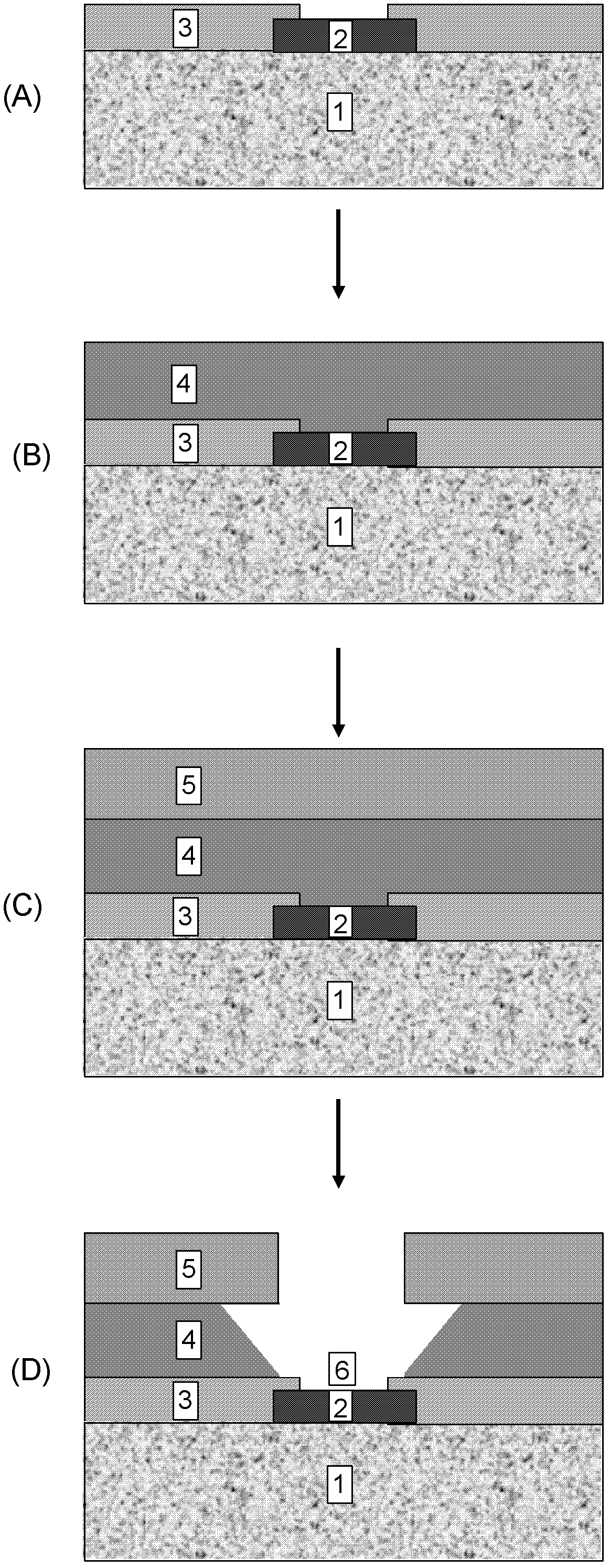
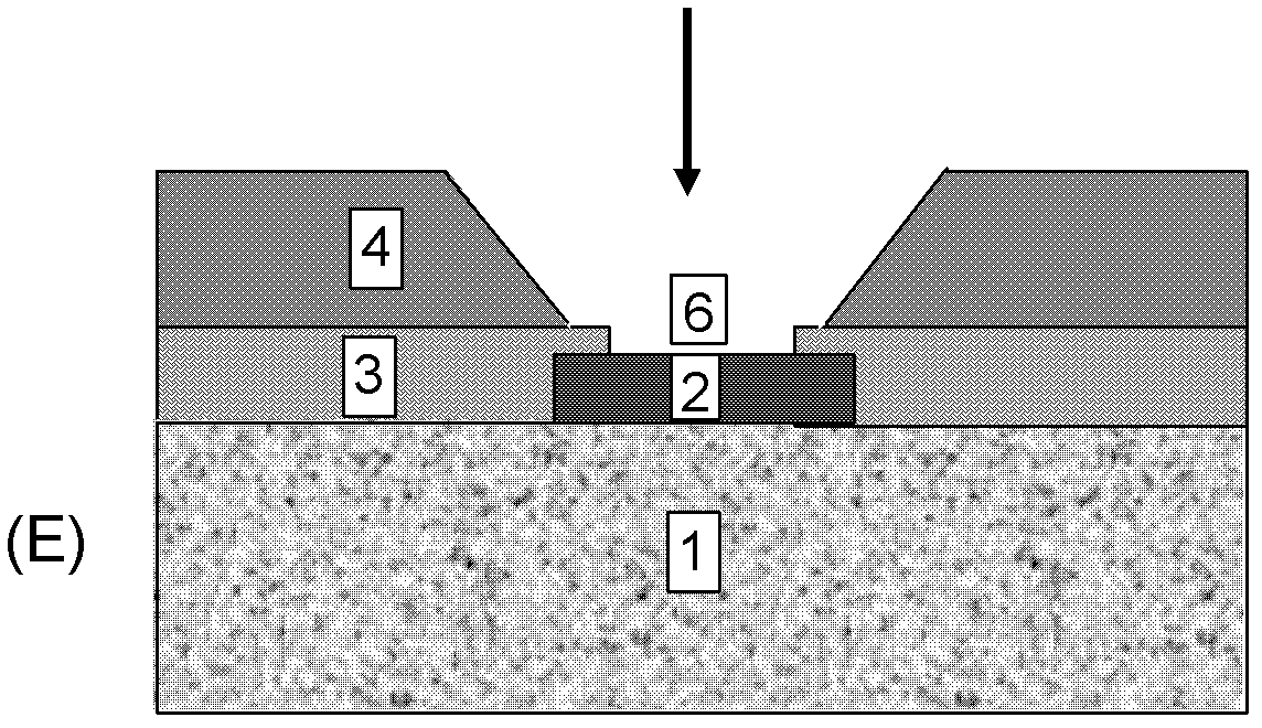
[0033] In order to have a more specific understanding of the technical content, characteristics and effects of the present invention, now in conjunction with the illustrated embodiment, the details are as follows:

[0034] Such as image 3 Shown, the preparation method of non-photosensitive polyimide passivation layer of the present invention, its main processing step is as follows:

[0035] Step 1, on semiconductor device 1, form the pattern of top layer metal aluminum line 2 and dielectric layer passivation film 3, as image 3 (A) shown. The dielectric layer passivation film 3 can be silicon nitride, silicon oxynitride, silicon dioxide or any combination thereof. According to the specific requirements of the process, the pattern of the passivation film 3 of the dielectric layer may not be formed.

[0036] Step 2, spin coating and baking a layer of non-photosensitive polyimide 4 with a thickness a (a is 1 to 50 microns) on the semiconductor device 1 on which the top layer ...


PUM

PropertyMeasurementUnit
Wavelengthaaaaaaaaaa
Thicknessaaaaaaaaaa
Thicknessaaaaaaaaaa

Abstract

The invention discloses a preparation method of a non-photosensitive polyimide passivation layer. The method comprises the following steps after a non-photosensitive polyimide spin coating step and before a solidifying step: 1) spin coating and baking a layer of photosensitive substances on the non-photosensitive polyimide; 2) conducting exposure and developing, removing the photosensitive substances of an exposure area, not removing or partially removing the non-photosensitive polyimide and partially forming non-photosensitive polyimide passivation layer holes; and 3) removing the photosensitive substances in the non-exposure area and the non-photosensitive polyimide in the passivation layer hole area in etching mode through a dry etching method. Due to the fact that the dry etching step is introduced in the preparation process of the non-photosensitive polyimide passivation layer, developing liquid cannot be directly contacted with an aluminum wire which is prevented from being corroded by the developing liquid in the developing process. Simultaneously, non-photosensitive polyimide passivation layers with different morphologies can be obtained to meet requirements for different product processes by controlling developing time.

Description

technical field [0001] The invention relates to the field of semiconductor integrated circuit manufacturing, in particular to a preparation method of a non-photosensitive polyimide passivation layer. Background technique [0002] Non-photosensitive polyimide (not photosensitive to any of the wavelengths of G-line (436 nm), I-line (365 nm), KrF (248 nm) and ArF (193 nm)) due to its Good high temperature resistance, mechanical properties, electrical properties and chemical stability have been widely used in the passivation layer process of semiconductor devices to reduce the damage caused by various natural environments and working environments to semiconductor devices and improve the reliability of devices. reliability and stability. [0003] The traditional non-photosensitive polyimide passivation layer preparation process such as figure 1 As shown, the main steps are: [0004] (1) Form top layer metal aluminum line 2 and dielectric layer passivation film 3 on semiconduct...

Claims


Application Information

Patent Timeline
IPC IPC(8): H01L21/312G03F7/20G03F7/00
Inventor 郭晓波程晋广
Owner SHANGHAI HUAHONG GRACE SEMICON MFG CORP
Why Eureka
Eureka Blog
Learn More