
Method of manufacturing printed circuit board, and printed circuit board obtained using method of manufacturing printed circuit board

A technology for printed circuit boards and manufacturing methods, which is applied in the fields of printed circuit manufacturing, printed circuits, and secondary treatment of printed circuits, etc., can solve problems such as difficulty in ensuring long-term reliability of printed circuit boards, surface layer movement, etc., and achieve excellent movement resistance, Excellent effect in terms of flat surface and stability in use

Active Publication Date: 2013-06-12
MITSUI MINING & SMELTING CO LTD
View PDF8 Cites 0 Cited by
  • Summary
  • Abstract
  • Description
  • Claims
  • Application Information

AI Technical Summary

Problems solved by technology

[0005] In addition, in the part where the delamination occurs, the surface layer movement due to the energization of the circuit is likely to occur, so it is difficult to ensure the long-term reliability of the printed circuit board.

Method used


Image

  • Method of manufacturing printed circuit board, and printed circuit board obtained using method of manufacturing printed circuit board
  • Method of manufacturing printed circuit board, and printed circuit board obtained using method of manufacturing printed circuit board
  • Method of manufacturing printed circuit board, and printed circuit board obtained using method of manufacturing printed circuit board

Examples


Embodiment 1

[0067] Manufacture of Copper Clad Laminates

[0068] On both sides of a material obtained by laminating three layers of prepreg (GHPL830-NS: manufactured by Mitsubishi Gas Chemical Co., Ltd.) with a thickness of 0.1mm, the non-rough surface roughness (ten-point average roughness Rzjis) of the overlapping pair is 0.37μm. Non-roughened copper foil with a primer resin layer (MFG-DMT3F: manufactured by Mitsui Metal Mining Co., Ltd.) made by coating copper foil with a primer resin, and then processed by a vacuum press at a temperature of 220°C and a pressure of 4.0MP. 90 minutes of forming to produce a copper clad laminate with a thickness of 0.3 mm.

[0069] Manufacturing of printed circuit boards

[0070] Printed circuit boards are manufactured using a semi-additive method. About the manufacturing process of this printed wiring board, an Example and a comparative example are common. Form an electroplating resist layer on the surface of the outer layer copper foil of the above-...

Embodiment 2

[0078] In Example 2, the non-roughened copper foil with a primer resin layer used in Example 1 was changed from MFG-DMT3F manufactured by Mitsui Metal Mining Co., Ltd. to PF-E-3 manufactured by Hitachi Chemical Industries, Ltd., except Otherwise, printed wiring board samples were produced in the same manner as in Example 1.

[0079]The above-mentioned printed wiring board sample was subjected to cleaning treatment in the same manner as in Example 1 to prepare a cleaning treatment sample, and semi-quantitative analysis was performed on the amount of residual metal components on the surface of the insulating resin layer exposed between circuits in the cleaning treatment sample. , and then determine the surface roughness (Rzjis). In addition, in the same manner as in Example 1, the occurrence of delamination was evaluated. The surface state of the insulating resin layer exposed between the circuits is shown in Table 1 below, and the evaluation results of delamination and cleanin...

Embodiment 3

[0081] In Example 3, using the sample of the printed wiring board produced in Example 1, only the cleaning treatment conditions were changed.

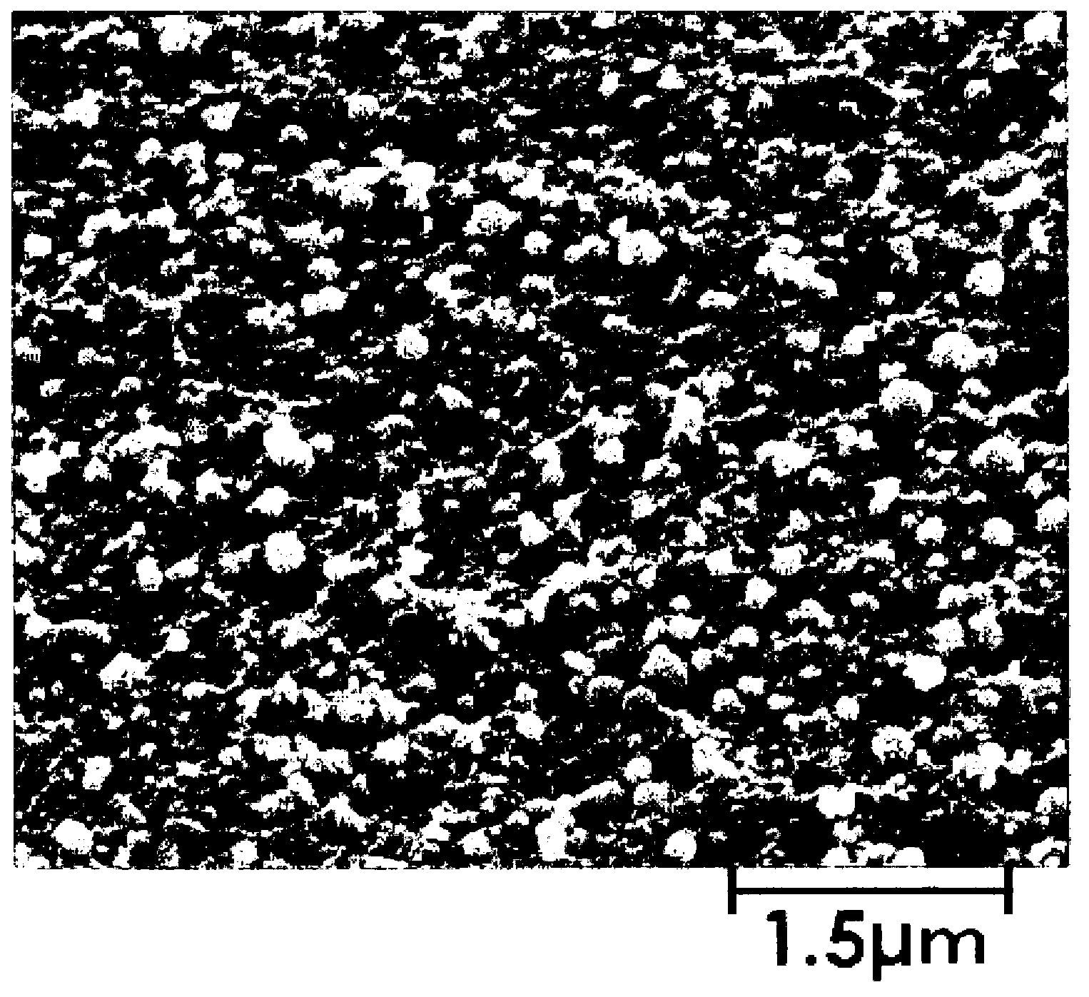
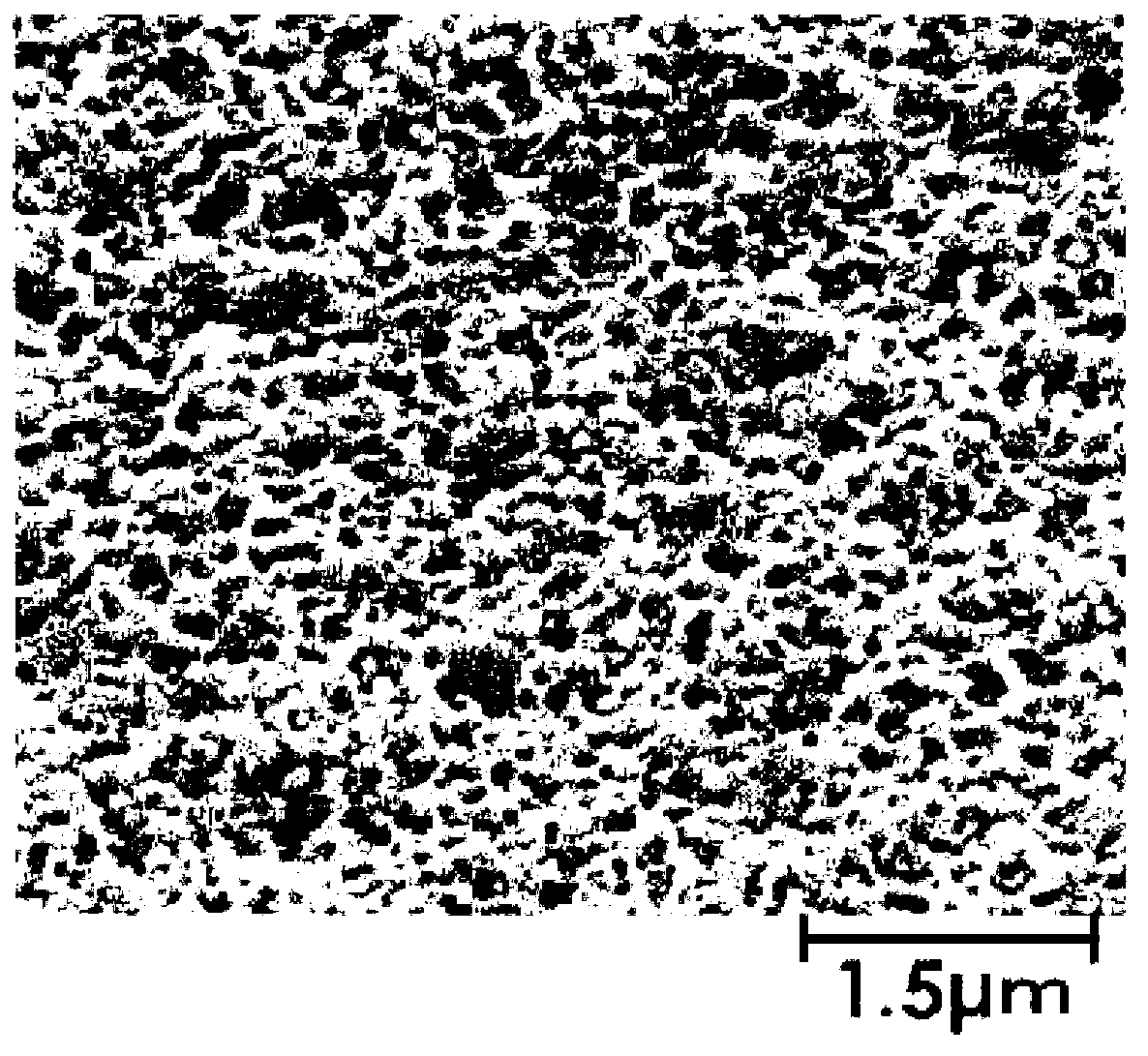
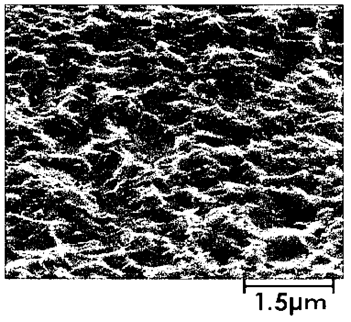
[0082] In the purification process, the sample of the above-mentioned printed circuit board was plasma etched under the condition of input energy of 40J / cm2 in a chamber of [(CF4 partial pressure) / (O2 partial pressure)]=0.33 and air pressure of 15Pa. Next, immerse for 5 minutes in a 10% by mass solution of sulfuric acid as an acid component and Melplate PC-316 (manufactured by Melplate Co., Ltd.) containing ethylene glycol as a surfactant, and after washing, spray a microetching solution (CZ8101B: manufactured by MEG Co., Ltd.) for 30 seconds, washed with water, and dried to prepare a purified sample. image 3 Shown is a scanning electron microscope observation image of the surface of the insulating resin layer exposed between the circuits immediately after the circuit is formed, figure 2 Shown is a scanning electron microscope obser...


PUM


Abstract

The objective of the present invention is to provide a method of manufacturing a printed circuit board having a good adhesion characteristic between faces of an insulation resin layer and a solder resist layer, even when the surface roughness of the insulation resin layer exposed between circuits is not so rough. In order to achieve this objective, a method of manufacturing a printed circuit board using a copper-clad laminate having non-roughened copper foils pasted together is adopted. The method of manufacturing a printed circuit board is characterized in forming circuits by etching the non-roughened copper foils with copper-etching liquid, then implementing cleanup processing on insulation resin surfaces exposed between the circuits, and characterized, upon conducting a semi-quantitative analysis of surface-treatment metal components of the non-roughened copper foils remaining on the insulation resin surfaces that had cleanup processing implemented thereupon, with an XPS analysis apparatus (X-ray source: A1(Ka), acceleration voltage: 15 kV, beam diameter: 50 [mu]m), in making the amount of each of the surface-treatment metal components to be not more than the detection limit.

Description

technical field [0001] The present invention relates to a method for manufacturing a printed wiring board and a printed wiring board obtained by the method for manufacturing a printed wiring board. In particular, it relates to a printed wiring board excellent in adhesiveness between a solder resist layer and an insulating resin layer surface exposed between circuits. Background technique [0002] Conventionally, the copper foil used in the production of copper-clad laminates has been obtained by roughening the bonding surface of the copper foil and the insulating resin layer, and forming irregularities of the roughening into the surface of the insulating resin layer. Physical fixation effect to bond insulating resin layers. Therefore, in the copper-clad laminate where the circuit is formed by etching and the copper foil layer is removed, the insulating resin layer having the irregularities transferred with the roughened shape is exposed. In the case of an insulating resin ...

Claims


Application Information

Patent Timeline
IPC IPC(8): H05K3/06H05K3/38
CPCH05K3/28H05K3/108H05K2203/0789
Inventor 吉川和广
Owner MITSUI MINING & SMELTING CO LTD
Learn More