Method for growing large-area graphene on insulating substrate

A technology on an insulating substrate and an insulating substrate, which is applied in the field of growing large-area graphene, can solve the problems of graphene size limitation, cumbersome process, and graphene performance degradation, so as to reduce production cost, high preparation repeatability, and external less disturbing effect

Inactive Publication Date: 2013-06-26
PEKING UNIV
View PDF1 Cites 22 Cited by
  • Summary
  • Abstract
  • Description
  • Claims
  • Application Information

AI Technical Summary

Problems solved by technology

[0003] Although the graphene obtained by the mechanical exfoliation method for preparing graphene proposed in 2005 has the highest quality of graphene reported now, the size of graphene obtained by this method is severely limited, generally only tens of microns size, and the cost and technical proficiency requirements of graphene prepared by this method are very high, which is only suitable for laboratory research and is not conducive to large-scale industrial growth (K.S.Novoselov et al., Nature438, 197.2005)
However, the process of this transfer step is quite cumbersome and requires high technology and proficiency of the transfer personnel.
At the same time, the pollution that may be introduced during the transfer process and the large amount of metal ions and organic macromolecules at the interface make the quality of graphene decline significantly in actual devices.

Method used


Image

  • Method for growing large-area graphene on insulating substrate
  • Method for growing large-area graphene on insulating substrate
  • Method for growing large-area graphene on insulating substrate

Examples


Embodiment 1

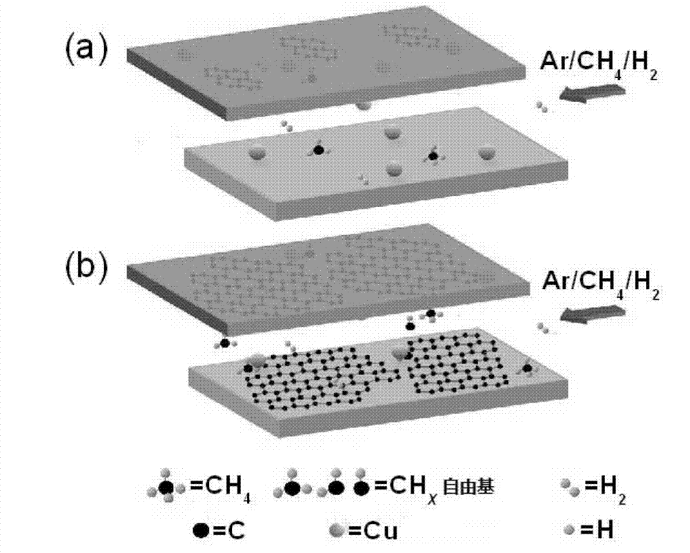
[0029] Example 1. Growth of large-scale single-layer graphene on (0001) sapphire substrate

[0030] 1) Use acetone to ultrasonically clean the sapphire (Kyocera, Japan) and copper foil (Alfa Aesar, UK) to remove organic residues, then use deionized water to ultrasonically remove metal ions and other impurities, and then quickly dry them with a nitrogen gun sample.

[0031] 2) Cover the (0001) sapphire on the copper foil and bring the two in close contact. Then push the entire sample into the central area of ​​the horizontal quartz tube furnace.

[0032] 3) The entire quartz tube of the tube furnace is cleaned three times with argon to remove the remaining impurity gas in the quartz tube.

[0033] 4) Before the temperature rise starts, argon gas of 100 sccm and hydrogen gas of 20 sccm are introduced, and the pressure is stabilized at 400 Pa by controlling the valve of the mechanical pump. Then raise the tube furnace to 1020°C within 50 minutes, and stabilize the growth temperature fo...


PUM

PropertyMeasurementUnit
thicknessaaaaaaaaaa
thicknessaaaaaaaaaa

Abstract

The invention discloses a method for growing large-area graphene on an insulating substrate. According to the method, a growing substrate is taken as an insulating material, a copper foil is taken as a catalyst and a carbon source, nitrogen and protective gas are taken as source gases, and the large-area graphene is grown on the insulating substrate by adopting a two-step (low-pressure growth and high-pressure growth) chemical vapor deposition method and using the short-range catalytic effect of the copper coil through face-to-face contact of the insulating substrate and the copper foil. The method disclosed by the invention is simple in operation of the whole process and low in cost; and the sample preparation is very high in repeatability and is less interfered by external world. The prepared single-layer graphene can be made into a large-area circuit device by using an exposure method without needing a complex transfer technology.

Description

Technical field [0001] The invention relates to a method for growing large-area graphene on an insulating substrate. Background technique [0002] Due to the discovery of the special Dirac electronic band structure and the bizarre fractional quantum Hall effect of graphene, two professors Konstantin Novoselov and Andre Geim from the University of Manchester won the 2010 Nobel Prize in Physics. At room temperature, the high carrier mobility and saturation velocity in graphene make graphene expected to replace silicon as the basic material for the next generation of large-scale integrated circuits. At this stage, the large-scale industrial application of graphene is mainly limited to the growth of graphene. In recent years, research on graphene growth, especially low-cost large-area growth, has attracted more and more attention from domestic and foreign companies, research institutes and university researchers. [0003] Although the graphene obtained by the mechanical exfoliation m...

Claims


Application Information

Patent Timeline
Patent Type & Authority Applications(China)
IPC IPC(8): C01B31/04C01B32/186
Inventor 陈建辉吴孝松施图万俞大鹏
Owner PEKING UNIV
Why Eureka
Try Eureka