

Preparation method of (doped amorphous) p-type transparent conductive oxide films
An amorphous thin film, transparent and conductive technology, applied in ion implantation plating, metal material coating process, coating and other directions, can solve the problems of low hole carrier concentration, poor room temperature conductivity, difficulty in the preparation of amorphous thin films, etc. , to achieve the effect of low deposition temperature, simple principle and low preparation cost
- Summary
- Abstract
- Description
- Claims
- Application Information
AI Technical Summary
Problems solved by technology
Method used
Image

Examples
Embodiment 1
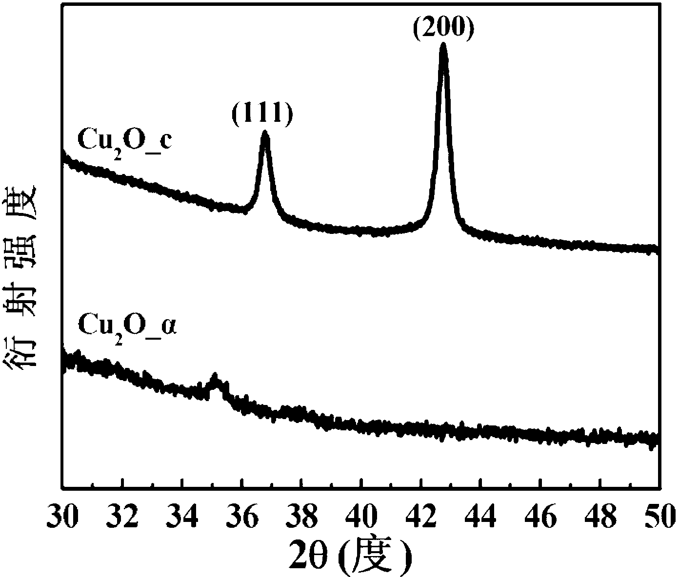
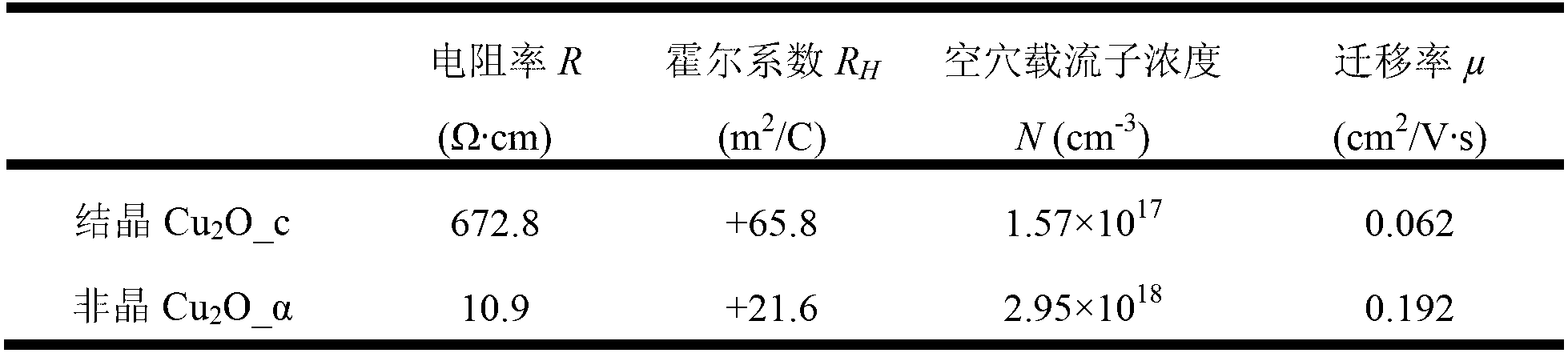
[0021] Prepare p-type transparent conductive amorphous cuprous oxide (Cu 2 O) film, specifically comprises the following steps:
[0022] Step 1: Prepare the substrate, first use acetone to ultrasonically clean the substrate for more than 10 minutes, then dry it, then use ethanol solution (analytical alcohol) to ultrasonically clean it for more than 10 minutes, and then dry it. The acetone ultrasonic cleaning and the ethanol solution ultrasonic cleaning are washed more than once each.
[0023] The substrate is a quartz substrate, and the thickness of the substrate is 0.5-2mm.
[0024] Step 2: Fix the substrate on the sample stage of the magnetron sputtering apparatus, and then put the sample stage into the vacuum chamber of the magnetron sputtering apparatus.
[0025] Step 3: Put the Cu target (purity greater than or equal to 99.99%) into the vacuum chamber and fix it on the target position.
[0026] Step 4: Vacuumize the vacuum chamber of the magnetron sputtering apparatus....
Embodiment 2
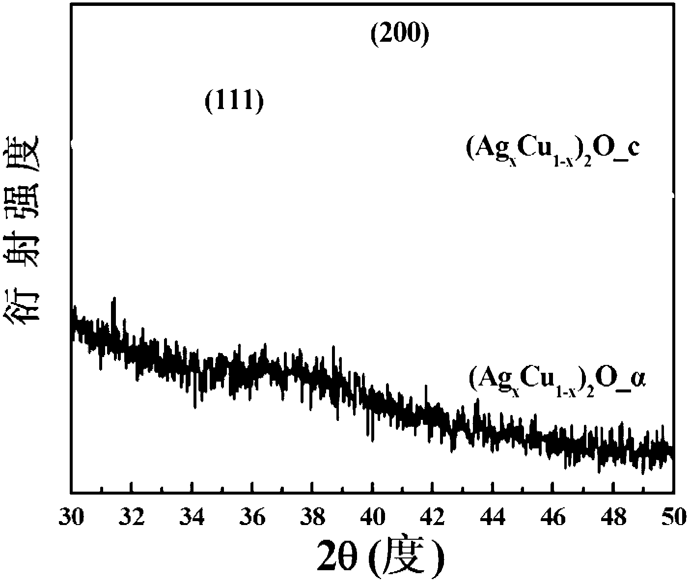
[0032] Prepare p-type transparent conductive Ag-doped cuprous oxide (Cu 2 O) amorphous thin film, specifically comprises the following steps:
[0033] Step 1: Prepare the substrate, first use acetone to ultrasonically clean the substrate for more than 10 minutes, then dry it, then use ethanol solution (analytical alcohol) to ultrasonically clean it for more than 10 minutes, and then dry it. The acetone ultrasonic cleaning and the ethanol solution ultrasonic cleaning are washed more than once each.
[0034] The substrate is a 7095 glass substrate, a quartz substrate or a NaCl single crystal substrate, and the thickness of the substrate is 0.5-2 mm.
[0035] Step 2: Fix the substrate on the sample stage of the magnetron sputtering apparatus, and then put the sample stage into the vacuum chamber of the magnetron sputtering apparatus.
[0036] Step 3: Put the Cu target (purity greater than or equal to 99.99%) into the vacuum chamber, fix it on the target position, and paste 6 pi...
Embodiment 3
[0043] Adopting the method provided by the invention to prepare Ag-doped cuprous oxide-based amorphous transparent conductive film comprises the following steps:
[0044] In the first step, NaCl single crystal substrates were prepared and cleaned alternately with acetone and ethanol by ultrasonic waves.
[0045] In the second step, the substrate is fixed on the sample stage of the magnetron sputtering apparatus, and then the sample stage is put into the vacuum chamber of the magnetron sputtering apparatus.
[0046] The third step is to put the Cu-Ag alloy target into the vacuum chamber and fix it on the target position, and the atomic percentage of Ag is less than or equal to 30%.
[0047] The fourth step, when the vacuum degree of the vacuum chamber reaches the predetermined value of 4.0~5.0×10 -4 After Pa, fill the vacuum chamber with high-purity O 2 gas and high-purity Ar gas to stabilize the gas pressure in the vacuum chamber at 1.0 to 2.0 Pa, wherein the gas pressure ra...
PUM
| Property | Measurement | Unit |
|---|---|---|
| thickness | aaaaa | aaaaa |
| electrical resistivity | aaaaa | aaaaa |
| electrical resistivity | aaaaa | aaaaa |
Abstract
Description
Claims
Application Information