Method for testing diffusion of boron to metal or metallic silicide of surface PMOS (p-channel metal oxide semiconductor) polysilicon gate
A metal silicide, surface channel technology, used in the semiconductor field
- Summary
- Abstract
- Description
- Claims
- Application Information
AI Technical Summary
Problems solved by technology
Method used
Image
Examples
Embodiment 1
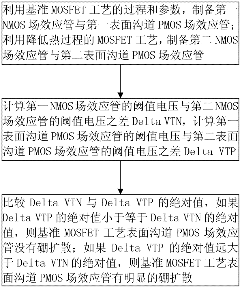
[0041] An embodiment of the method for determining the diffusion of surface channel PMOS polysilicon gate boron to metal or metal silicide figure 1 shown, including the following steps:
[0042] 1. Utilize the process and parameters of the benchmark MOSFET process to prepare the first NMOS field effect transistor and the first surface channel PMOS field effect transistor; wherein, the NMOS field effect transistor uses N-type polysilicon as the gate electrode, and the PMOS uses boron ( B) P-type polysilicon as gate electrode;
[0043] The second NMOS field effect transistor and the second surface channel PMOS field effect transistor are prepared by using the MOSFET process to reduce the thermal process;
[0044] Compared with the benchmark MOSFET process, the MOSFET process with reduced thermal process has lower temperature and / or shorter time of thermal process after the gate preparation process, and other processes and parameters are the same; the better MOSFET process with re...
Embodiment 2
[0054] Based on Embodiment 1, the benchmark MOSFET process includes the following steps:
[0055] 1. Active region preparation;
[0056] 2. Double well ion implantation;
[0057] 3. Threshold voltage adjustment injection;
[0058] 4. MOS device gate oxide layer growth;
[0059] 5. Gate preparation, wherein the surface channel PMOS gate adopts P-type polysilicon doped with boron (B);
[0060] 6. Polysilicon oxidation;
[0061] 7. Lightly doped drain (LDD) implantation and rapid thermal annealing;
[0062] 8. Silicon nitride or silicon oxide sidewall CVD deposition;
[0063] 9. Source-drain injection and rapid thermal annealing;
[0064] 10. Preparation of self-aligned metal silicide;
[0065] 11. Back metal connection.
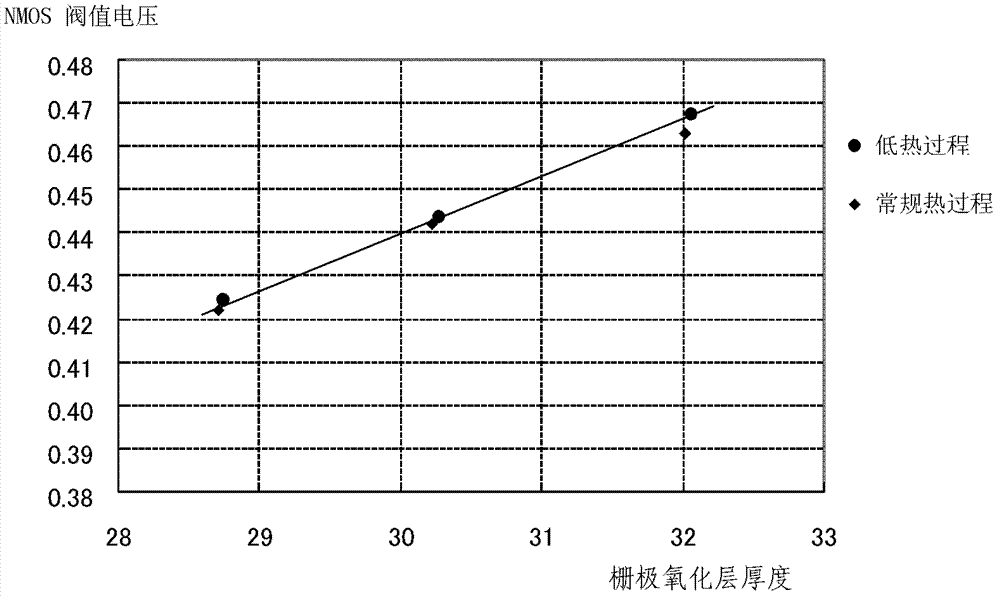
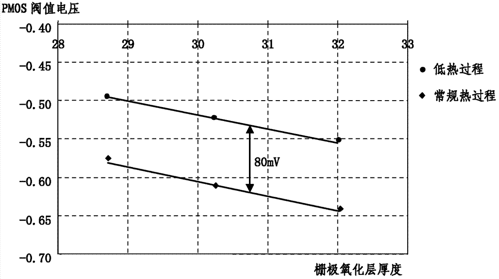
[0066] figure 2 Shown is the threshold voltage VTN(A) of the first NMOS field effect transistor and the threshold voltage VTN(B) of the second NMOS field effect transistor. It can be seen that the threshold voltage VTN(A) of the first NMOS field effec...
PUM
 Abstract
Description
Claims
Application Information
 - R&D
- Intellectual Property
- Life Sciences
- Materials
- Tech Scout
- Unparalleled Data Quality
- Higher Quality Content
- 60% Fewer Hallucinations
Browse by: Latest US Patents, China's latest patents, Technical Efficacy Thesaurus, Application Domain, Technology Topic, Popular Technical Reports.
© 2025 PatSnap. All rights reserved.Legal|Privacy policy|Modern Slavery Act Transparency Statement|Sitemap|About US| Contact US: help@patsnap.com


