Thin film transistor

A technology of thin film transistor and etching barrier layer, applied in the direction of transistor, etc., can solve the problems of short circuit of thin film transistor, poor reliability of thin film transistor, influence of working performance of thin film transistor, etc., and achieve the effect of improving reliability

Active Publication Date: 2013-07-03
海宁经开产业园区开发建设有限公司
View PDF8 Cites 6 Cited by
  • Summary
  • Abstract
  • Description
  • Claims
  • Application Information

AI Technical Summary

Problems solved by technology

However, materials such as copper or aluminum are prone to diffusion or electron migration during use
When metal atoms such as copper or aluminum diffuse into the channel layer, it will affect the performance of the thin film transistor, and even cause a short circuit of the thin film transistor
Therefore, the above-mentioned thin film transistors have poor reliability

Method used


Image

  • Thin film transistor
  • Thin film transistor

Examples


Embodiment Construction

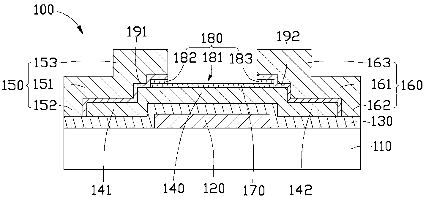
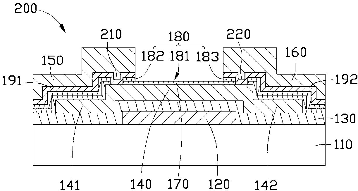
[0012] See figure 1 , the thin film transistor 100 provided by the first embodiment of the present invention includes a substrate 110, a gate 120, a gate insulating layer 130, a channel layer 140, a source 141, a drain 142, a source electrode 150, a drain electrode 160, a first The etch stop layer 170 and the second etch stop layer 180 . Wherein, the manufacturing material of the substrate 110 is selected from glass, quartz, silicon wafer, polycarbonate, polymethyl methacrylate or metal foil.

[0013] The gate 120 is disposed on the surface of the substrate 110 . In this embodiment, the gate 120 is disposed in the central area of ​​the substrate 110 . The gate electrode 120 is made of copper, aluminum, nickel, magnesium, chromium, molybdenum, tungsten and alloys thereof.

[0014] The gate insulating layer 130 covers the surface of the gate 120 . In this embodiment, the gate insulating layer 130 extends to contact with the substrate 110 . The gate insulating layer 130 is m...


PUM


Abstract

The invention discloses a thin film transistor which comprises a substrate, a gate arranged on the substrate, a gate insulation layer covering the gate and an active layer covering the gate insulation layer, wherein the active layer comprises a trench layer, a source and a drain; the source and the drain are respectively arranged on two opposite sides of the trench layer and are electrically connected with a corresponding source electrode and a corresponding drain electrode; a first etching barrier layer and a second etching barrier layer are sequentially arranged on the surface of the trench layer; a groove for exposing the first etching barrier layer is formed in the middle of the second etching barrier layer and divides the second etching barrier layer into a first region and a second region; the source electrode extends from the surface of the source to cover the first region; and the drain electrode extends from the surface of the drain to cover the second region. By the structure, the influence caused by metal atom dispersion or electron migration of the source electrode or the drain electrode on the conductive performance of the trench layer can be effectively prevented; and the reliability is improved.

Description

technical field [0001] The invention relates to a thin film transistor. Background technique [0002] With the advancement of process technology, thin film transistors have been widely used in displays to meet the requirements of thinning and miniaturization of displays. Thin film transistors generally include components such as gate, drain, source, and channel layer, which change the conductivity of the channel layer by controlling the voltage of the gate, so that the source and drain are turned on or off. state. [0003] Generally, thin film transistors often use copper or aluminum as the material for making the source electrode or the drain electrode. However, materials such as copper or aluminum are prone to diffusion or electron migration during use. When metal atoms such as copper or aluminum diffuse into the channel layer, it will affect the performance of the thin film transistor, and even cause a short circuit of the thin film transistor in severe cases. Therefo...

Claims


Application Information

Patent Timeline
IPC IPC(8): H01L29/786
Inventor 曾坚信
Owner 海宁经开产业园区开发建设有限公司
Why Eureka
Try Eureka