High voltage light-emitting diode and manufacturing method thereof

A high-voltage light-emitting and diode technology, which is applied in the direction of electrical components, electric solid-state devices, circuits, etc., can solve the problems of LED active area damage, long time, and reduced working life, and achieve the effect of reducing etching depth and reducing damage

Inactive Publication Date: 2013-07-03
INST OF SEMICONDUCTORS - CHINESE ACAD OF SCI
View PDF8 Cites 9 Cited by
  • Summary
  • Abstract
  • Description
  • Claims
  • Application Information

AI Technical Summary

Problems solved by technology

However, in this prior art solution, such as figure 1 , since the epitaxial layer is to be etched from the p-type layer 13 to the sapphire substrate 10, it is necessary to etch an isolation deep groove 101 with a depth of 4-7um, so that the interconnection line 20 between each LED unit 100 is due to climbing through such Deep isolation grooves 101 lead to poor reliability, which leads to low yield of high-voltage LED chips, and greatly reduces the working life under high voltage, while the deep etching process and the thickened e

Method used


Image

  • High voltage light-emitting diode and manufacturing method thereof
  • High voltage light-emitting diode and manufacturing method thereof
  • High voltage light-emitting diode and manufacturing method thereof

Examples


Embodiment 1

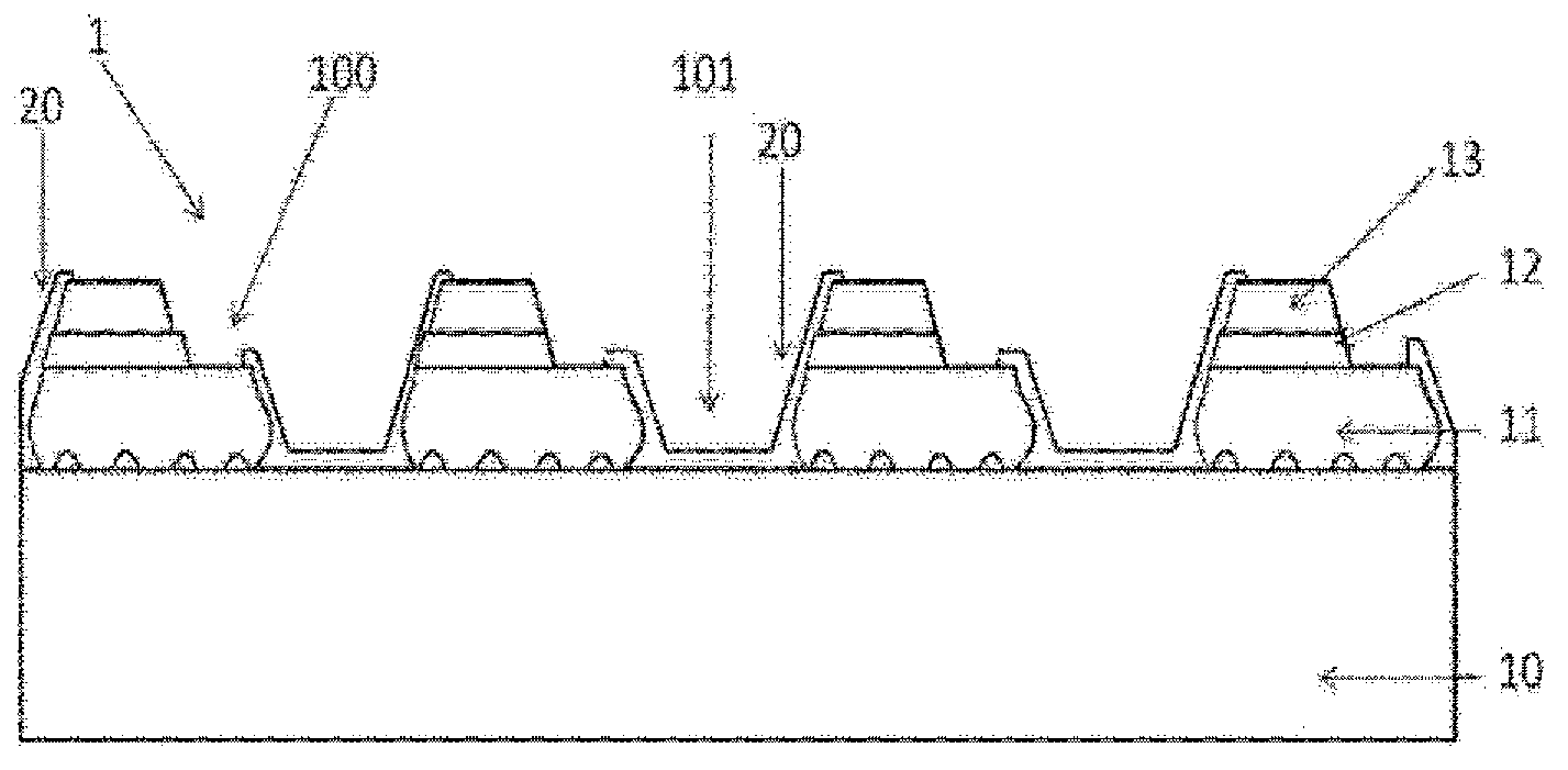
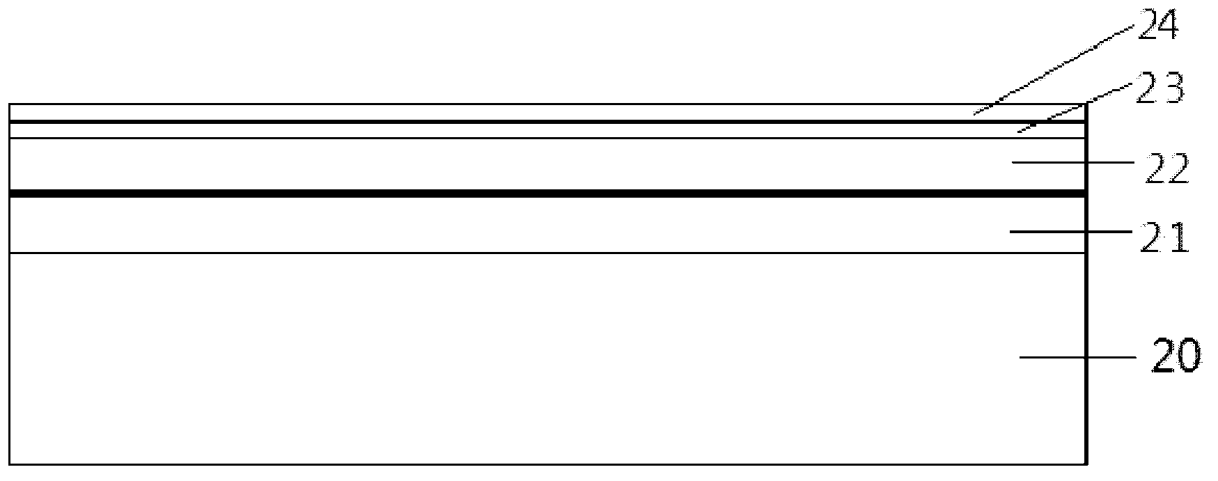
[0035] Use MOCVD equipment to form an AlN buffer layer on the c-surface of the sapphire substrate. The thickness of the AlN buffer layer is 1.2um; on the AlN buffer layer, sequentially form an n-type GaN layer of about 3um and a GaN / InGaN multiple quantum well with a thickness of 100-200nm layer and a 100-300nm thick p-type GaN layer.

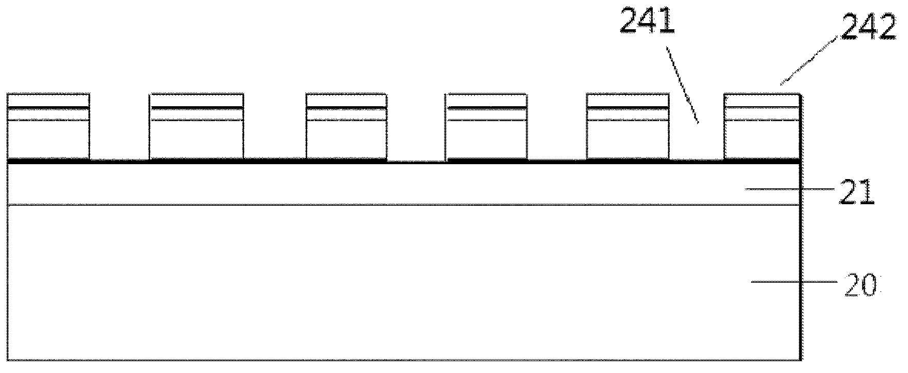
[0036] After the epitaxial wafer is cleaned, an ITO transparent electrode layer is formed by electron beam evaporation on the p-type GaN layer. After patterning, ICP etches the mesa to expose the n-type GaN layer; PECVD silicon oxide can also be used as a masking layer for etching trenches. Mask the photoresist to form an isolation trench with a depth of about 3.5um between the LED light-emitting units; after removing the masking layer, photolithography forms the p and n electrode solder joint areas and metal interconnection areas, and uses electron beam evaporation of CrPtAu to form p , n-electrode solder joints and metal interconnection lines, ...


PUM

PropertyMeasurementUnit
Thicknessaaaaaaaaaa

Abstract

The invention relates to a manufacturing method of a high voltage light-emitting diode. The manufacturing method of the high voltage light-emitting diode comprises the steps of forming an insulating buffer layer on a substrate; forming an n-type semiconductor layer, an active layer and a p-type semiconductor layer on the insulating buffer layer; patterning the n-type semiconductor layer, the active layer and the p-type semiconductor layer, then etching the n-type semiconductor layer, the active layer and the p-type semiconductor layer to form grooves till the insulating buffer layer is exposed out of the bottoms of the grooves, forming a plurality of isolated luminous units through the grooves; and forming metal interconnecting wires, and connecting the adjacent luminous units in series. The manufacturing method is characterized in that the grooves are 2.5mu m-4mu m deep. By adopting the manufacturing method of the high voltage light-emitting diode, the damages to the active area of LED (light-emitting diode), which are caused by the long-term plasma bombardment, are reduced, and the luminous degree of LED is improved.

Description

technical field [0001] The invention relates to a high-voltage flip-chip light-emitting diode chip. More specifically, the present invention relates to a high-voltage LED chip structure with an insulating buffer layer and a manufacturing method thereof. Background technique [0002] Light-emitting diodes (LEDs) have the advantages of long life, energy saving, environmental protection, and rich colors. Therefore, with the development of technologies such as epitaxy, chips, and packaging, and the further improvement of luminous efficiency, LEDs have been gradually used in lighting, display, medical treatment, etc. each field. Traditional gallium nitride-based light-emitting diodes work under DC voltage, the voltage range is 2.9-3.5V, and the working current is usually 20mA. In order for light-emitting diodes to achieve the brightness required for general lighting, the operating current of the LED chip must generally be increased to more than 100mA. Currently, 100mA, 350mA an...

Claims


Application Information

Patent Timeline
IPC IPC(8): H01L33/00H01L33/20H01L27/15
Inventor 郭金霞闫建昌伊晓燕田婷詹腾赵勇兵宋昌斌王军喜
Owner INST OF SEMICONDUCTORS - CHINESE ACAD OF SCI
Why Eureka
Try Eureka