Multilayer dual-gate graphene field effect transistor and preparation method for same

A field-effect transistor, single-layer graphene technology, applied in semiconductor/solid-state device manufacturing, semiconductor devices, electrical components, etc., can solve the problems of unreached, small drain-source current, small heat capacity, etc. The effect of mobility

Inactive Publication Date: 2013-07-17
XIDIAN UNIV
View PDF3 Cites 19 Cited by
  • Summary
  • Abstract
  • Description
  • Claims
  • Application Information

AI Technical Summary

Problems solved by technology

However, due to the defects of the material itself and the influence of various scattering mechanisms, the carrier mobility in graphene is far from reaching its intrinsic value, so there is still room for further improvement in the high-frequency characteristics of graphene.
[000

Method used


Image

  • Multilayer dual-gate graphene field effect transistor and preparation method for same
  • Multilayer dual-gate graphene field effect transistor and preparation method for same
  • Multilayer dual-gate graphene field effect transistor and preparation method for same

Examples


Embodiment

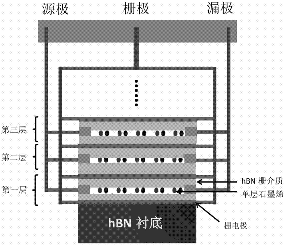
[0056] A three-layer double-gate graphene field-effect transistor is fabricated and tested by the method of the invention.

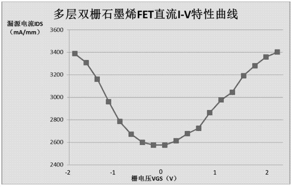
[0057] Such as figure 2 Shown is the transfer characteristic curve diagram of the three-layer double-gate graphene field-effect transistor, and it can be drawn that by stacking three double-gate graphene transistors together, the obtained three-layer double-gate graphene field-effect transistor is The drain-source current at the same gate voltage is nearly three times higher than that of a single double-gate graphene transistor.

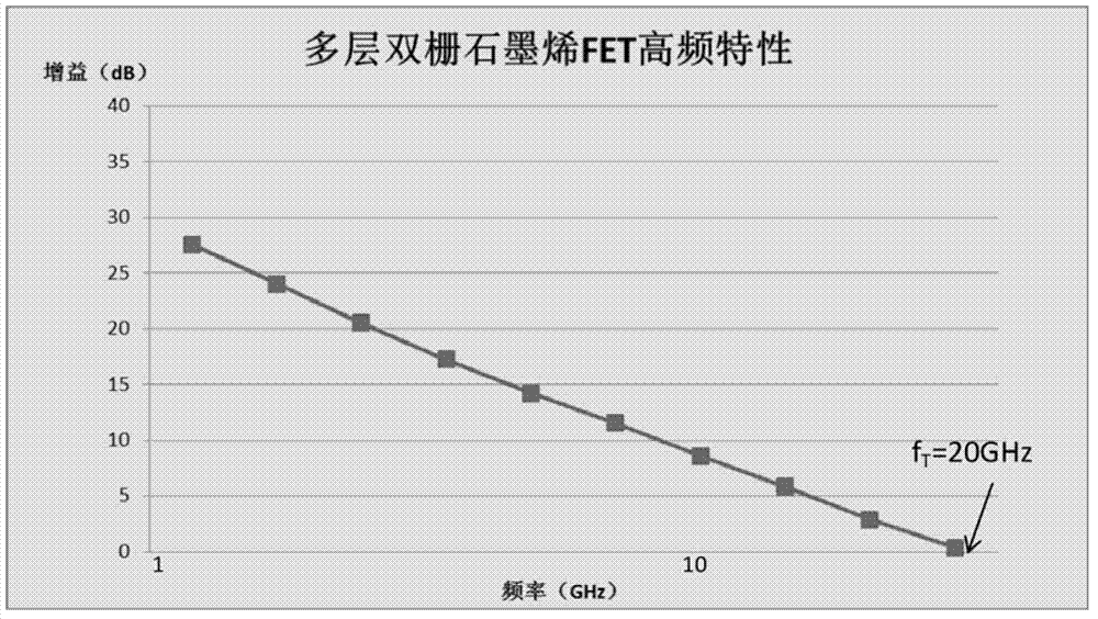
[0058] Such as image 3 Shown is the high-frequency characteristic curve of the three-layer double-gate graphene field effect transistor. It can be concluded that the high-frequency characteristics of the device are not degraded compared with a single double-gate graphene transistor, and the dielectric frequency reaches 200 GHz. It shows that, through the structure and method of the present invention, the power characteristi...


PUM

PropertyMeasurementUnit
Thicknessaaaaaaaaaa
Thicknessaaaaaaaaaa
Thicknessaaaaaaaaaa

Abstract

The invention discloses a multilayer dual-gate graphene field effect transistor. The multilayer dual-gate graphene field effect transistor comprises a hexagonal boron nitride substrate, a source electrode, a drain electrode, a bottom gate metal electrode deposited on the substrate, a back gate medium, single-layer graphene, a top gate medium and a top gate metal electrode, wherein the bottom gate metal electrode is connected with the top gate metal electrode. In case of a plurality of layers of transistors, the transistors are connected in parallel, and the drain and source electrodes of the transistors are connected in parallel respectively. The multilayer dual-gate graphene field effect transistor has the advantage that hexagonal boron nitride is used as the top gate medium and the bottom gate medium, is a two-dimensional planar material, and has a few surface dangling bonds and trapped charges, so that the migration rate of carriers of a graphene channel can be increased. According to the multilayer dual-gate graphene field effect transistor, the drain and source current of the graphene field effect transistor can be maximally improved, and the graphene field effect transistor is widely applied to the field of high-frequency high-power devices.

Description

technical field [0001] The invention relates to a field effect transistor device and a preparation process thereof, in particular to a field effect transistor device using graphene as a channel material and a preparation process thereof. Background technique [0002] Graphene is considered to be a new field-effect transistor channel material with great potential. Graphene is a two-dimensional film material formed by carbon atoms in a hexagonal lattice, in which sp 2 The σ bonds formed by hybridization are connected. Graphene has very excellent electrical properties, and the low-temperature intrinsic mobility of carriers is as high as 200,000 cm 2 / Vs. At present, the mobility of the manufactured graphene field effect transistor is 3000cm 2 / Vs to 10000cm 2 / Vs or so, the cutoff frequency reaches 100GHz. However, due to the defects of the material itself and the influence of various scattering mechanisms, the carrier mobility in graphene is far from reaching its intrins...

Claims


Application Information

Patent Timeline
IPC IPC(8): H01L29/78H01L21/336
Inventor 马中发张鹏吴勇庄奕琪肖郑操赵钰迪郭超冯元博
Owner XIDIAN UNIV
Why Eureka
Try Eureka