

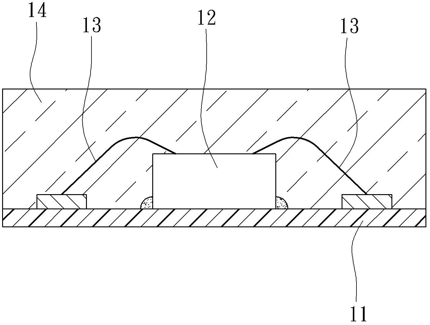
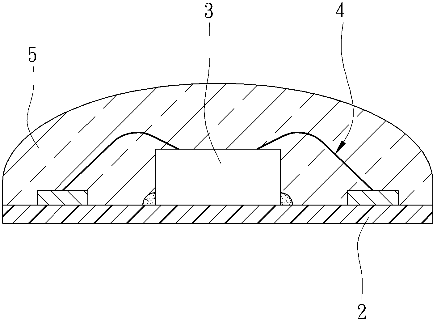
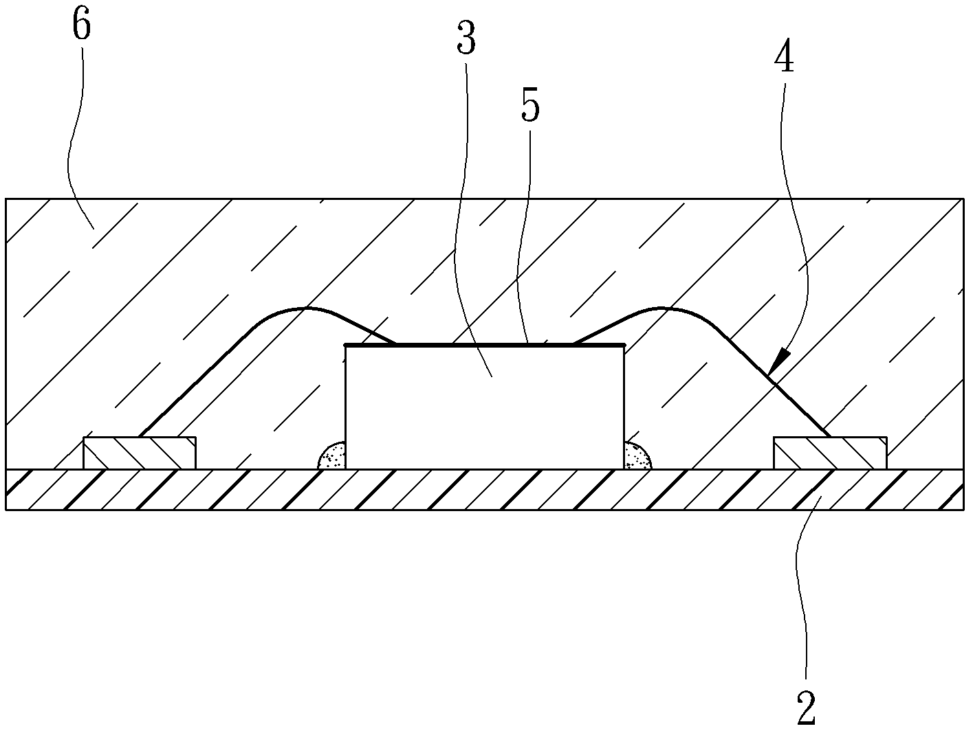
High-transmittance packaged LED (light emitting diode)
A technology of light-emitting diodes and high transmittance, applied in electrical components, electrical solid devices, circuits, etc., can solve the problems of low mechanical strength, large difference in refractive index, low brightness, etc., and achieve the effect of good luminous efficiency
- Summary
- Abstract
- Description
- Claims
- Application Information
AI Technical Summary
Problems solved by technology
Method used
Image

Examples
preparation example 1
[0044] (a) 258g of vinyl chloride (purchased from Formosa Plastics) was added to 15000g of silane (Silane, purchased from Germany Waker, model 62M) and 3 / 1000 catalyst potassium hydroxide (KOH), stirred and mixed at a temperature of 120 for 30 15250g of vinyl silicon-based material (Vinylsilicone) can be obtained in 1 minute. Because during the reaction process, part of the materials involved in the reaction are consumed, so the weight will decrease.
[0045] (b) Add 15,000 g of vinyl silicon-based materials to 236 g of epoxy silane (purchased from Waker, Germany, model S510), and stir and mix at a temperature of 25° C. for 10 minutes to obtain 15,236 g of A glue. At this time, the vinyl bonded silicon-based material and the epoxy silane do not react with each other. The chemical formula of this epoxy silane is as follows:
[0046]
[0047](c) 15000g of hydrogen-bonded silicon-based material (Hydroxysilicone, purchased from Waker, Germany, model 62M) was added to 102g of ...
preparation example 2
[0050] (a) With the method described in (a) of , 15250 g of vinyl bonded silicon-based materials were obtained.
[0051] (b) Add 15,000 g of vinyl silicon-based materials to 220 g of epoxy silane (purchased from Waker, Germany, model S520), and stir and mix at a temperature of 25° C. for 10 minutes to obtain 15,236 g of A glue. At this time, the vinyl bonded silicon-based material and the epoxy silane do not react with each other. The chemical formula of this epoxy silane is as follows:
[0052]
[0053] (c) With the method described in (c) of , obtain the B glue of 15102g.
[0054] (d) Add 15220 g of glue A to 15102 g of glue B and stir and mix at a temperature of 25° C. for 10 minutes to make glue A and glue B polymerize and obtain 30322 g of a copolymer. The copolymer has 0.73% epoxysilane.
preparation example 3
[0056] (a) With the method described in (a) of , 15250 g of vinyl bonded silicon-based materials were obtained.
[0057] (b) Add 15,000 g of the vinyl bonded silicon-based material to 736 g of epoxy silane, stir and mix at a temperature of 25° C. for 10 minutes to obtain 15,736 g of A glue. At this time, the vinyl bonded silicon-based material and the epoxy silane do not react with each other. The chemical formula of this epoxy silane is as follows:
[0058]
[0059] (c) With the method described in (c) of , obtain the B glue of 15102g.
[0060] (d) Add 15736g of glue A to 15102g of glue B and stir and mix at a temperature of 25°C for 10 minutes to make glue A and glue B polymerize and obtain 30838g of copolymer. The copolymer has 2.38% epoxysilane.
PUM
 Abstract
Description
Claims
Application Information