Method for manufacturing vertical multi-junction solar cell piece by laser
A technology of solar cells and vertical multi-junctions, which is applied in the manufacture of circuits, electrical components, and final products, and can solve the problems of numerous processes, complex processes, and high processing costs
- Summary
- Abstract
- Description
- Claims
- Application Information
AI Technical Summary
Problems solved by technology
Method used
Image

Examples
Embodiment 1
[0041] Sample: Intrinsic single crystal silicon wafer.
[0042] Impurity atmosphere used: Phosphine (PH 3 ) gas (n-type), diborane (B 2 h 6 ) gas (p type), pressure 0.1bar.
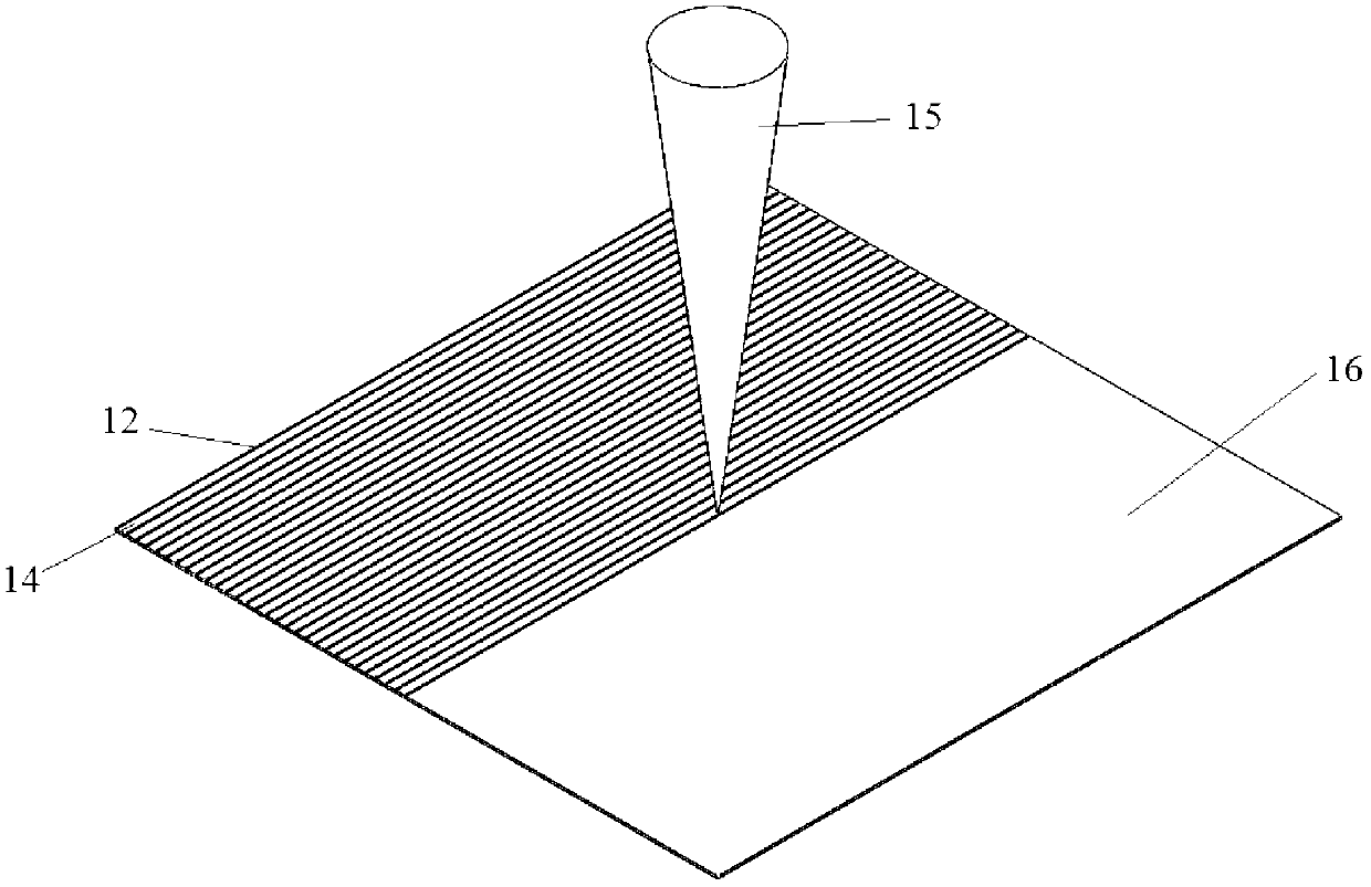
[0043] Processing parameters: laser wavelength 790nm, repetition frequency 1kHz, pulse width 150fs, focusing objective lens 4 magnification 10, platform moving speed 100μm / s, doped stripe width 100μm, doped stripe intrinsic area width 300μm.
[0044] The specific steps are:
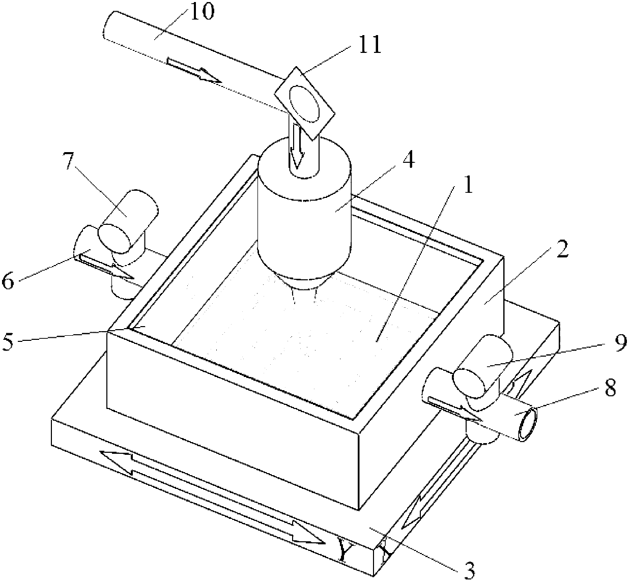
[0045] 1. Make the thickness 200μm and the area 50×50mm 2 The intrinsic single crystal wafer (1) is placed in the center of the vacuum chamber (2), and the semiconductor material (1) is rotated so that the X direction and Y direction of the three-dimensional mobile platform are parallel to the oriented side of the semiconductor material; the semiconductor material is fixed; as figure 1 shown;
[0046] 2. Close the inlet valve 7, open the outlet valve 9, connect the outlet 8 to a vacuum pump (not shown in the figure), vacuumize ...
Embodiment 2
[0054] The laser wavelength is 532nm, the repetition frequency is 500kHz, the pulse width is 100ps, the laser power is 2W, the magnification of the focusing objective lens is 4, the moving speed of the platform is 1mm / s, the width W of the doped stripe is 50μm, and the width of the intrinsic region of the doped stripe is W i 0μm, the thickness of the silicon wafer is 200μm, and the area is 50×50mm 2 monocrystalline silicon wafers. The impurity atmosphere used is diborane (B 2 h 6 ) gas (p-type).
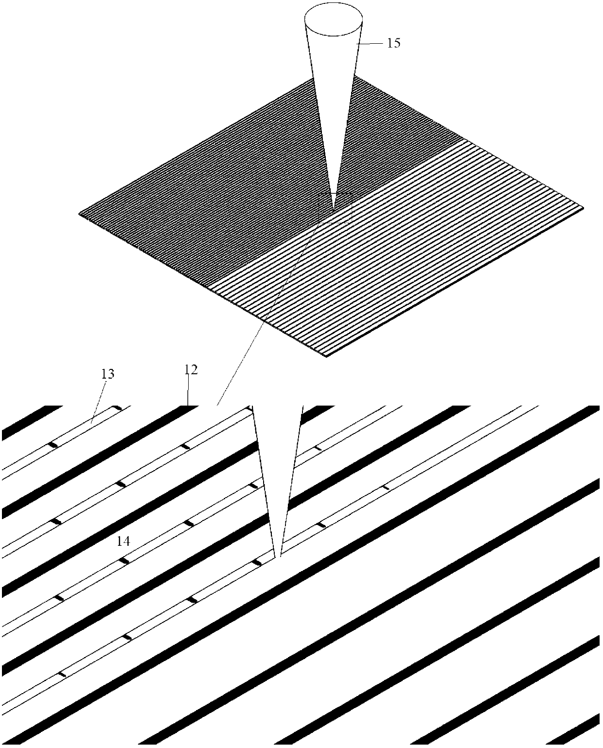
[0055] The specific steps are the same as in Embodiment 1, except that the moving length S is 100 mm, the translation distance of two adjacent linear movements is 15 μm, and the period of the doped stripe sequence is 150 μm. The rear electrode grooves have a width of 70 μm and a depth of 100 μm.
Embodiment 3
[0057] The laser wavelength is 1064nm, the repetition frequency is 500kHz, the pulse width is 100ps, the laser power is 5W, the magnification of the focusing objective lens is 20, the moving speed of the platform is 10mm / s, the width of the doped stripe is 5μm, and the width of the intrinsic region of the doped stripe is 50μm. The silicon wafer is 200μm in thickness and 50×50mm in area 2 n-type intrinsic polysilicon wafer. The impurity atmosphere used is phosphine (PH 3 ) gas (n-type) and diborane (B 2 h 6 ) gas (p-type).
[0058] The specific steps are the same as in Example 1, except that each doped stripe is formed by one scan, the moving length S is 500 mm, the translation distance of two adjacent linear movements is 10 μm, and the period of the doped stripe sequence is 120 μm. The width of the rear electrode groove is 10 μm and the depth is 50 μm.
PUM
 Abstract
Description
Claims
Application Information
 - R&D
- Intellectual Property
- Life Sciences
- Materials
- Tech Scout
- Unparalleled Data Quality
- Higher Quality Content
- 60% Fewer Hallucinations
Browse by: Latest US Patents, China's latest patents, Technical Efficacy Thesaurus, Application Domain, Technology Topic, Popular Technical Reports.
© 2025 PatSnap. All rights reserved.Legal|Privacy policy|Modern Slavery Act Transparency Statement|Sitemap|About US| Contact US: help@patsnap.com