Square wave detector for wireless wake-up circuit
A wake-up circuit and detector technology, applied in the field of radio frequency electronics, can solve the problems of reducing wake-up time, high cost of printed circuit board design, and complex peripheral circuit structure
- Summary
- Abstract
- Description
- Claims
- Application Information
AI Technical Summary
Problems solved by technology
Method used
Image
Examples
no. 1 example
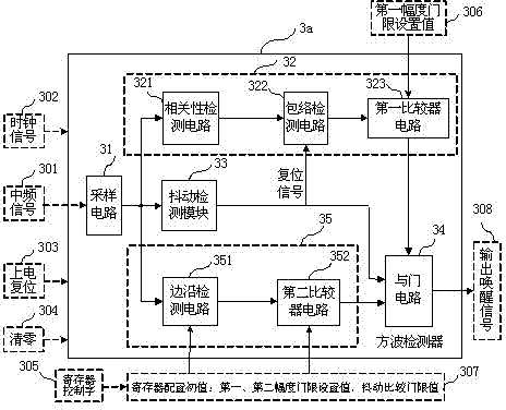
[0077] Figure 3a Provide the structural block diagram of the 14kHz square wave detector that N is 14 in the first embodiment of the present invention applied in the ETC system, as Figure 3a As shown: the square wave detector 3 a includes a sampling circuit 31 , a correlation detection module 32 , a jitter detection module 33 , a frequency detection module 35 and an AND gate circuit 34 . The correlation detection module 32 includes a correlation detection circuit 321 , an envelope detection circuit 322 and a first comparator circuit 323 sequentially connected in series. The frequency detection module 35 includes an edge detection circuit 351 and a second comparator circuit 352 . The output end of the jitter detection module 33 and the output end of the second comparator circuit 352 of the frequency detection module 35 are respectively connected to an input end of the AND gate circuit, and the output end of the first comparator circuit 323 of the correlation detection module ...
no. 2 example
[0079] Figure 3b It is a structural block diagram of a 14kHz square wave detector with N being 14, which is applied in the ETC system according to the second embodiment of the present invention. Such as Figure 3b As shown: the square wave detector includes a sampling circuit 31 , a correlation detection module 32 , a jitter and frequency detection module 36 combined by a jitter detection circuit and a frequency detection circuit, and an AND circuit 34 . The correlation detection module 32 includes a correlation detection circuit 321 , an envelope detection circuit 322 and a first comparator circuit 323 sequentially connected in series. The jitter detection module and the frequency detection module are combined into a jitter and frequency detection module 36 , which includes a jitter detection circuit 361 , an edge detection circuit 362 , and a second comparator circuit 363 . The output ends of the jitter detection circuit 361 and the edge detection circuit 362 are respecti...
no. 3 example
[0081] The schematic block diagram of the circuit composition of the correlation detection module is as follows: Figure 4 shown. The correlation detection module is composed of cross-correlation operation mixers 411 and 412 , a digital oscillator 413 , two cross-correlation integration and accumulation circuits 42 and 43 , an envelope detection circuit 322 and a first comparator circuit 323 . The integration and accumulation circuit 42 includes a first integrator circuit 421 and a first accumulator circuit 422 connected in series; the integration and accumulation circuit 43 includes a second integrator circuit 431 and a second accumulator circuit 432 connected in series; the second integrator The output of circuit 431 is applied to the input of first integrator circuit 421 . The circuit connection of the correlation detection module path is as follows: the output terminal of the digital oscillator 413 is connected with the local oscillator signal input terminals of the two-w...
PUM
 Abstract
Description
Claims
Application Information


