Growing method of GaN-based light-emitting diode extensional structure

A technology of light-emitting diodes and epitaxial structures, applied in the direction of electrical components, circuits, semiconductor devices, etc., can solve the problems affecting the brightness of epitaxial wafers, affecting the antistatic ability, etc., to improve surface morphology, reduce V-shaped defects, improve Effect of Crystal Quality

Active Publication Date: 2013-07-31
宁波安芯美半导体有限公司
View PDF3 Cites 15 Cited by
  • Summary
  • Abstract
  • Description
  • Claims
  • Application Information

AI Technical Summary

Problems solved by technology

The internal stress in the active layer will affect the internal quantum efficiency of the epitaxial wafer and the brightness of the epitaxial wafer, and also affect the antistatic ability

Method used


Image

  • Growing method of GaN-based light-emitting diode extensional structure
  • Growing method of GaN-based light-emitting diode extensional structure
  • Growing method of GaN-based light-emitting diode extensional structure

Examples


Embodiment Construction

[0023] The embodiments of the present invention are described in detail below: the present embodiment is implemented under the premise of the technical solution of the present invention, and detailed implementation and specific operation process are provided, but the protection scope of the present invention is not limited to the following implementation example.

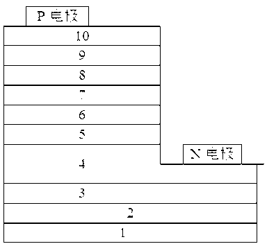
[0024] like figure 1 The LED epitaxial structure shown includes, from bottom to top, substrate 1, low-temperature GaN buffer layer 2, GaN undoped layer 3, N-type GaN layer 4, shallow quantum well layer 5, light-emitting quantum well layer 6, A low-temperature P-type GaN layer 7 , a PAIGaN current blocking layer 8 , a high-temperature P-type GaN layer 9 , and a P-type contact layer 10 .

[0025] The method for growing the above-mentioned LED epitaxial structure includes the following specific steps:

[0026] Step 1: Clean the substrate 1 at a high temperature for 5-20 minutes in a hydrogen atmosphere at 1000-1200°C...


PUM


Abstract

The invention discloses a growing method of a GaN-based light-emitting diode extensional structure. The extensional structure disclosed by the invention comprises a substrate, a low-temperature GaN buffering layer, a GaN non-doped layer, an N-type GaN layer, a light quantum well layer, a light-emitting quantum well layer, a low-temperature P-type GaN layer, a PAlGaN current blocking layer, a high-temperature P-type GaN layer and a P-type contact layer in sequence from bottom to top, wherein the light quantum well layer comprises a plurality of quantum well structures overlapped in sequence; the quantum well structures are formed by growing InxGa1-xN potential well layers, wherein x is greater than 0 and smaller than 1 and GaN barrier layers sequentially grow with a gradient growth rate; and a Ga source extensionally grow by using TMGa or TEG A. by adopting the growing method disclosed by the invention, the crystal quality, the light-emitting efficiency and the luminance can be better improved.

Description

[0001] technical field [0002] The invention relates to the technical field of preparation of GaN-based light-emitting diode (LED) materials, in particular to an epitaxial growth method of a GaN-based light-emitting diode shallow quantum well layer. [0003] Background technique [0004] During the growth process of the epitaxial layer of gallium nitride-based InGaN / GaN multiple quantum well light-emitting diodes, due to lattice mismatch and epitaxial film deposition defects and other reasons, GaN-based light-emitting diode materials will generate stress during the growth process. The internal stress in the active layer will affect the internal quantum efficiency of the epitaxial wafer and the brightness of the epitaxial wafer, and will also affect the antistatic ability. [0005] In a typical epitaxial layer structure, the shallow well layer is interposed between the N-type GaN layer and the light-emitting quantum well layer, and this layer plays a major role in epitax...

Claims


Application Information

Patent Timeline
Patent Type & Authority Applications(China)
IPC IPC(8): H01L33/00H01L33/32H01L33/06
Inventor 郭丽彬刘仁锁蒋利民李刚
Owner 宁波安芯美半导体有限公司
Why Eureka
Try Eureka