Nonvolatile memory element, production method therefor, nonvolatile memory unit, and design assistance method for nonvolatile memory element

一种非易失性存储、制造方法的技术,应用在非易失性存储元件及其制造领域,能够解决妨碍电阻变化元件初始化等问题,达到维持导电性、抑制接触电阻的增加、漏电流减少的效果

Active Publication Date: 2013-07-31
PANASONIC SEMICON SOLUTIONS CO LTD
View PDF5 Cites 5 Cited by
  • Summary
  • Abstract
  • Description
  • Claims
  • Application Information

AI Technical Summary

Problems solved by technology

Therefore, when a conductive path is formed on the transition metal oxide (resistance change film) of the resistance change element after manufacture, a voltage whose absolute value is higher than the usual drive voltage for resistance change is applied once to several times. In the initialization of the variable resistance film, compared with the case of having small protrusions on the electrode, the initialization voltage (initialization voltage) needs to be higher, which hinders initialization at a low voltage in the variable resistance element.
[0018] In addition, although the initializing voltage can be lowered if the film thickness of the second variable resistance layer is reduced, it is not desirable from the viewpoint of reliability.

Method used


Image

  • Nonvolatile memory element, production method therefor, nonvolatile memory unit, and design assistance method for nonvolatile memory element
  • Nonvolatile memory element, production method therefor, nonvolatile memory unit, and design assistance method for nonvolatile memory element
  • Nonvolatile memory element, production method therefor, nonvolatile memory unit, and design assistance method for nonvolatile memory element

Examples


Embodiment approach 1

[0101] First, the nonvolatile memory element in Embodiment 1 of the present invention will be described.

[0102] [constitute]

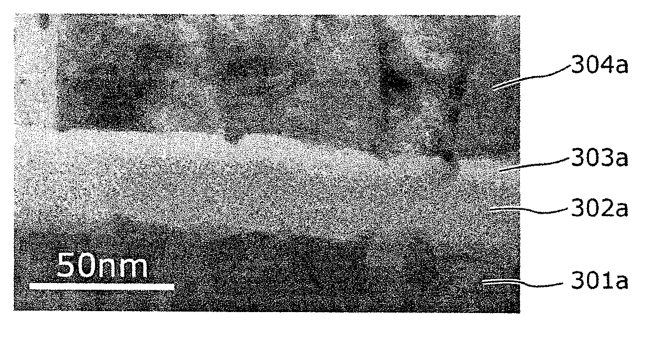
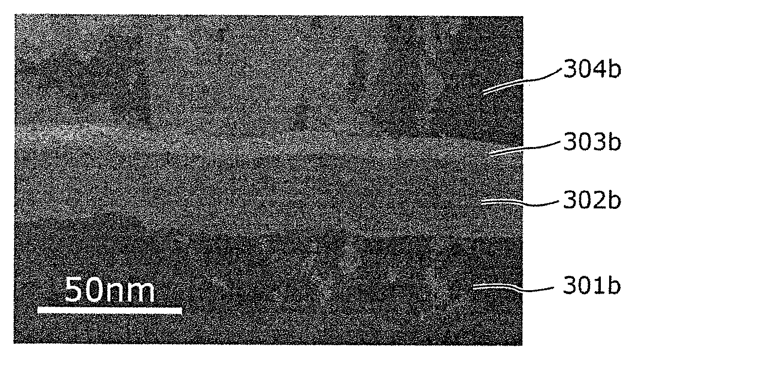
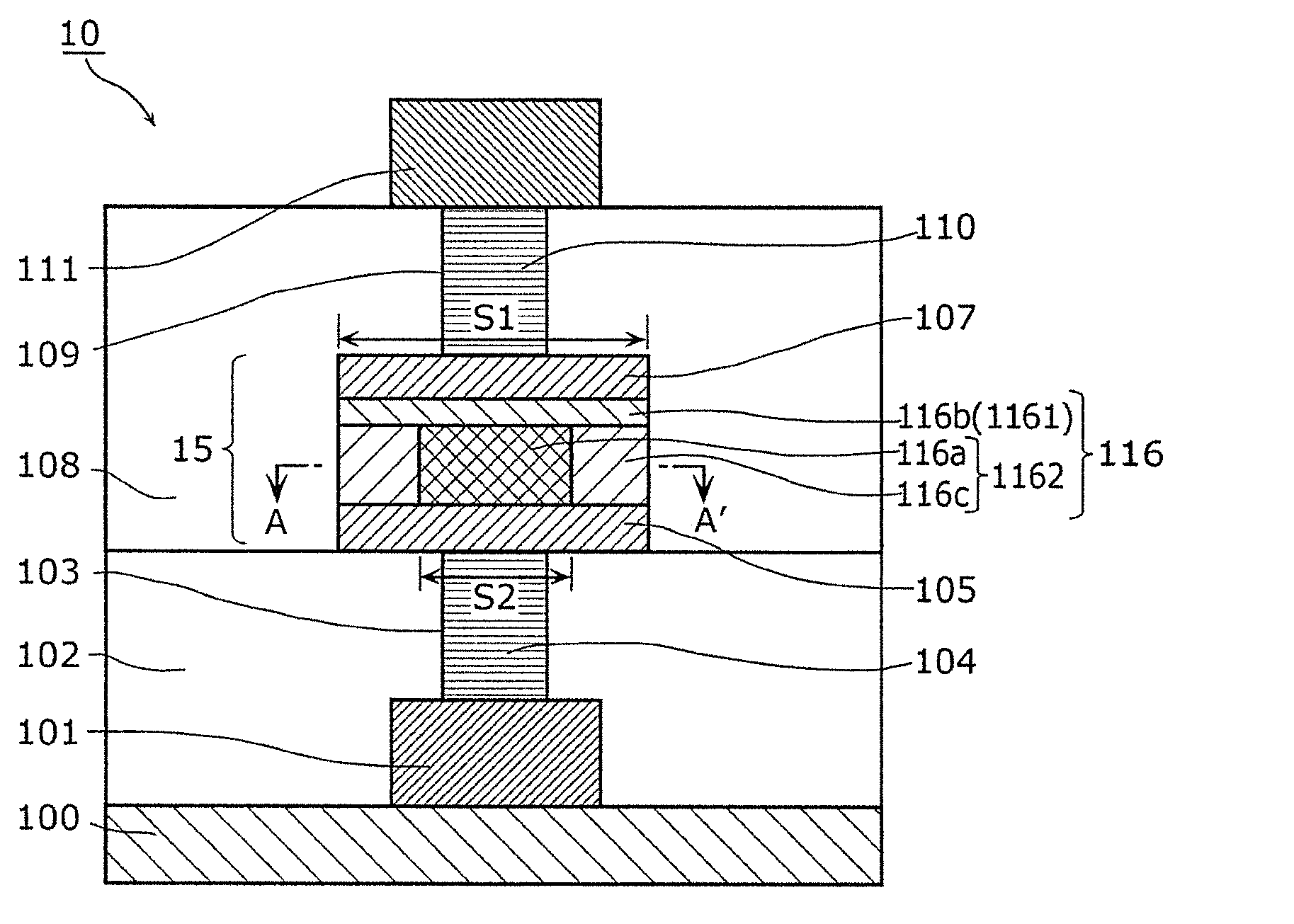
[0103] Figure 2A It is a sectional view of the nonvolatile memory element 10 according to Embodiment 1 of the present invention. Figure 2B yes Figure 2A Sectional view of line AA' in . Such as Figure 2A As shown, the nonvolatile memory element 10 of this embodiment is a variable resistance nonvolatile memory element, and includes a substrate 100, a first wiring 101, a first interlayer insulating layer 102, a first contact plug 104, a resistor The variable element 15 , the second interlayer insulating layer 108 , the second contact plug 110 and the second wiring 111 . Furthermore, when an actual memory cell is configured using the nonvolatile memory element 10 of this embodiment, either one of the first wiring 101 and the second wiring 111 is connected to a switching element (diode or transistor), and It is determined that the switching elem...

Embodiment approach 2

[0152] Next, the nonvolatile memory element in Embodiment 2 of the present invention will be described.

[0153] [constitute]

[0154] Figure 14A It is a sectional view of the nonvolatile memory element 20 according to Embodiment 2 of the present invention. Figure 14B is looking in the direction of the arrow Figure 14A A cross-sectional view of the section of the line BB' in the figure. Such as Figure 14A As shown, the nonvolatile memory element 20 of the second embodiment is a variable resistance nonvolatile memory element, and includes a substrate 100 made of silicon (Si), a first wiring 101, a first interlayer insulating layer 102, The first contact plug 104 , the variable resistance element 25 , the second interlayer insulating layer 108 , the second contact plug 110 , and the second wiring 111 .

[0155] The variable resistance element 25 is composed of a lower electrode 105 , a variable resistance layer 126 , and an upper electrode 107 . The variable resistance...

Embodiment approach 3

[0169] Next, the nonvolatile memory element in Embodiment 3 of the present invention will be described.

[0170] [constitute]

[0171] Figure 16 It is a sectional view of the nonvolatile memory element 30 in Embodiment 3 of the present invention. Such as Figure 16 As shown, the nonvolatile memory element 30 of this embodiment is a variable resistance nonvolatile memory element, and includes a substrate 100 such as silicon (Si), a first wiring 101, a first interlayer insulating layer 102, a first 1. Contact plug 104, variable resistance element 35, second interlayer insulating layer 108, second contact plug 110, and second wiring 111. The variable resistance element 35 is composed of a lower electrode 105 , a variable resistance layer 136 , and an upper electrode 107 . The variable resistance layer 136 is interposed between the lower electrode 105 and the upper electrode 107, and reversibly changes the resistance value based on an electric signal applied between the two e...


PUM


Abstract

This nonvolatile memory element is provided with a resistance change layer (116) which is interposed between a bottom electrode (105) and an upper electrode (107) and in which the resistance value reversibly varies on the basis of electrical signals applied between both of the electrodes. The resistance change layer (116) includes at least two layers that are a first resistance change layer (1161) and a second resistance change layer (1162). The first resistance change layer (1161) contains a first transition metal oxide (116b). The second resistance change layer (1162) contains a second transition metal oxide (116a) and a transition metal compound (116c). The oxygen content of the second transition metal oxide (116a) is lower than that of the first transition metal oxide (116b). The transition metal compound contains oxygen and nitrogen, or oxygen and fluorine. The second transition metal oxide (116a) and the transition metal compound (116c) are in contact with the first resistance change layer (1161).

Description

technical field [0001] The present invention relates to a nonvolatile memory element, a manufacturing method thereof, a nonvolatile memory device, and a design support method for a nonvolatile memory element, and in particular, to a device capable of changing its resistance by application of an electric pulse. A variable resistance nonvolatile memory element having a variable resistance layer in which the resistance value is changed and the changed resistance value is maintained, and a method for manufacturing the same. Background technique [0002] In recent years, with the development of digital technology, electronic devices such as portable information devices and information home appliances have been further functionalized. Therefore, there are increasing demands for increasing the capacity, reducing the writing power, speeding up the writing / reading time, and increasing the lifetime of the nonvolatile memory element. [0003] Contrary to such a request, it can be said...

Claims


Application Information

Patent Timeline
Patent Type & Authority Applications(China)
IPC IPC(8): H01L27/105G11C11/15G11C29/56H01L45/00H01L49/00
CPCG11C2213/34H01L27/02H01L45/1675H01L27/101G11C2213/55H01L45/1233H01L45/1641H01L27/2436G11C2213/32H01L45/146G11C13/0007H01L27/24H01L27/2427H01L45/08H01L45/1625H10B63/30H10N70/24H10N70/826H10N70/8833H10N70/026H10N70/041H10N70/063H10B63/24
Inventor 早川幸夫三河巧二宫健生
Owner PANASONIC SEMICON SOLUTIONS CO LTD
Why Eureka
Try Eureka