Chip package structure and device

A chip packaging and chip technology, which is applied to antenna supports/installation devices, instruments, resonant antennas, etc., and can solve the problems of high loss of packaging materials and low manufacturing resolution.

Active Publication Date: 2013-08-14
TESSERA INC
View PDF5 Cites 49 Cited by
  • Summary
  • Abstract
  • Description
  • Claims
  • Application Information

AI Technical Summary

Problems solved by technology

However, for operating frequencies in the 94GHz and even higher bands, the use of the above organic or ceramic based multilayer antenna structures is problemati

Method used


Image

  • Chip package structure and device
  • Chip package structure and device
  • Chip package structure and device

Examples


Embodiment Construction

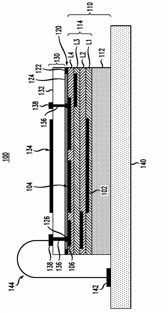
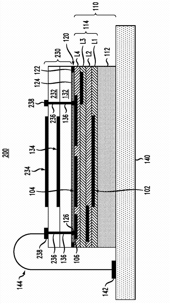
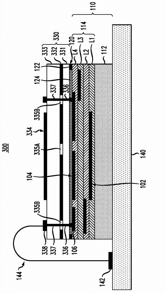
[0020] Exemplary embodiments of the present invention will now be described in further detail with reference to a wafer-scale packaging structure and method that integrates a packaged antenna structure with a semiconductor RFIC (radio frequency integrated circuit) chip to form a mm wave) applications (e.g., 94GHz) and terahertz (THz) applications (e.g., 300GHz to 6THz) compact integrated radio / wireless communication systems. In general, a package structure according to an exemplary embodiment of the present invention includes an antenna structure fabricated using a silicon or thin film fabrication process that is integrated with an RFIC chip using wafer-scale fabrication techniques. will refer to below Figure 1-12 In the exemplary embodiment of the package structure described in detail, the package structure generally includes an RFIC (radio frequency integrated circuit) chip, an antenna structure and an interface layer. An RFIC chip includes a semiconductor substrate having...


PUM


Abstract

The invention relates to a chip package structure and a device. Wafer-scale packaging structures and methods are provided for integrally packaging antenna structures with semiconductor RFIC (radio frequency integrated circuit) chips to form compact integrated radio/wireless communications systems for millimeter wave (mmWave) and Terahertz (THz) applications. For example, a chip package includes an RFIC chip, an antenna structure and an interface layer. The RFIC chip includes a semiconductor substrate having an active surface and an inactive surface, and a BEOL (back end of line) structure formed on the active surface of the semiconductor substrate. The antenna structure includes an antenna substrate and a planar antenna radiator formed on a surface of the antenna substrate, wherein the antenna substrate is formed of a low loss semiconductor material. The interface layer connects the antenna structure to the BEOL structure of the RFIC chip.

Description

technical field [0001] The present invention generally relates to wafer-scale packaging structures with integrated antennas. More specifically, it relates to wafer-scale packaging structures and methods for integrally packaging antenna structures with semiconductor RFIC (radio frequency integrated circuit) chips, thereby forming compact packages for millimeter wave (mm wave) and terahertz (THz) applications. Integrated radio / wireless communication system. Background technique [0002] In a wireless network, connectivity and communication between devices is achieved using antennas coupled to receivers or transmitters to transmit desired signals to and from other elements of the network. In traditional radio communication systems (e.g. mmWave radios), discrete components are often assembled with a low level of integration. These systems are often assembled using expensive and bulky waveguides and package-level or board-level microstrip structures to interconnect semiconducto...

Claims


Application Information

Patent Timeline
IPC IPC(8): H01L23/31H01Q1/38H01Q1/22H01L23/66G06K19/077
CPCH01L2224/13025H01L23/66H01L2924/1421H01L24/13G06K19/07775H01L2924/15192H01L2224/73253H01L2924/15311H01Q1/2283H01L27/14618H01L2224/0401H01Q1/38H01L2224/48091H01L23/5225H01L2224/32225H01Q9/0407H01Q1/22G06K19/077H01L2924/19104H01L24/48H01L24/32H01L23/5227H01L2224/48227H01L2924/19107H01L2224/04042H01L23/31H01L2223/6627H01L24/16H01L2224/05009H01L2224/16225H01L2223/6677H01L2224/73265H01L24/73H01L2224/451H01L2924/00014H01L2924/00H01L2224/45099H01L2224/05599
Inventor 刘兑现J-O·普卢沙尔S·K·雷诺兹
Owner TESSERA INC
Why Eureka
Try Eureka