Method for preparing metal nano-circular ring

A technology of metal nanoparticles and metal nanoparticles, applied in nanotechnology, electrical components, circuits, etc., can solve the problems of high cost, low production efficiency, and difficult preparation of metal nano rings, and achieve the effect of simple preparation

Active Publication Date: 2013-08-28
INST OF SEMICONDUCTORS - CHINESE ACAD OF SCI
View PDF4 Cites 4 Cited by
  • Summary
  • Abstract
  • Description
  • Claims
  • Application Information

AI Technical Summary

Problems solved by technology

[0003] However, the preparation of metal nanorings is more difficult than that of disc-shaped metal nanoparticles
At present, the preparation of metal nanocircles is mainly carried out by advanced photolithography techniques such as electron beam lithography. However, the significant disadvantages of electron beam lithography are high cost and low production efficiency.

Method used


Image

  • Method for preparing metal nano-circular ring
  • Method for preparing metal nano-circular ring
  • Method for preparing metal nano-circular ring

Examples


Embodiment Construction

[0017] In order to make the purpose, technical scheme and advantages of the present invention clearer, the present invention will be described in detail below in conjunction with the accompanying drawings and specific examples, specifically providing the preparation of metal nano-rings composed of a single metal material and metal nano-rings composed of two metals. Two examples of metallic nanocircles.

[0018] Taking the LED structure in the visible light band as an example, metal nano-rings can be grown inside the N-type GaN film, inside the electron blocking layer, inside the P-type GaN film and on the surface of the P-type GaN. The two embodiments of the metal nano-circle manufacturing method given below are both illustrated by growing a metal nano-circle on the surface of P-type GaN as an example.

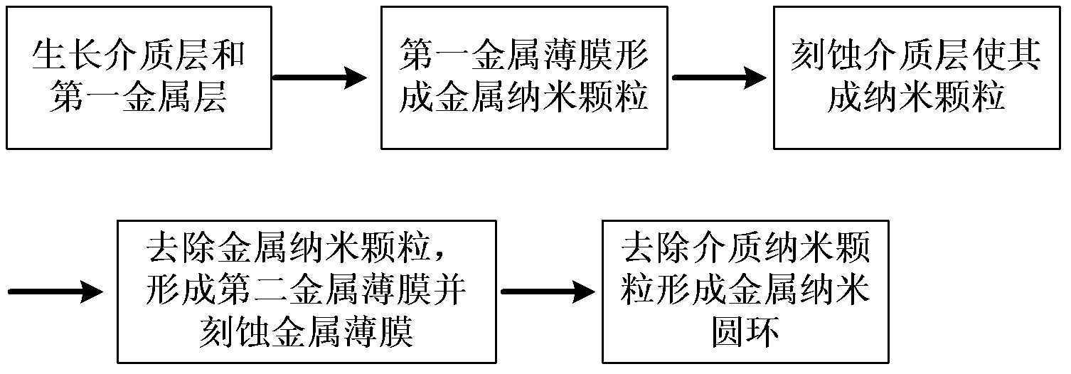
[0019] image 3 A flow chart of the preparation method of the metal nanocircle proposed by the present invention is shown. Such as image 3 As shown, the preparation method...


PUM


Abstract

The invention discloses a method for preparing a metal nano-circular ring. The method comprises a first step of sequentially planting a medium layer and a first metal layer on the surface of a thin film of a photoelectric device, wherein the metal nano-circular ring needs to be formed on the surface of the thin film, a second step of machining a first metal thin film into metal nano-particles through the annealing process, a third step of etching the medium layer to form medium nano-particles with the metal nano-particles as a reticle mask, a fourth step of removing the metal nano-particles, planting at least one layer of a second metal thin film on the device surface provided with the medium nano-particles and on the tops and the side walls with the medium nano-particles, etching the second metal thin film, and only retaining the second metal thin film on the side walls with the medium nano-particles, and a fifth step of removing the medium nano-particles and finally forming the metal nano-circular ring.

Description

technical field [0001] The invention relates to an optoelectronic device, in particular to a preparation method of a metal nano-circle that can improve LED luminous efficiency. Background technique [0002] Nano-metal plasmonic technology has been proved experimentally to be a technology that can effectively improve the luminous efficiency of LEDs. At present, the commonly used metal nanostructures are disk-shaped nanostructures, and the properties of metal plasmons can be adjusted mainly by adjusting the type of metal material and the radius of the nanodisk to meet the requirements of optoelectronic systems. There are two kinds of metal ring structures, including nano-rings 100 made of a metal material, such as figure 1 As shown, and a nano-ring 200 composed of two metal materials, such as figure 2 shown. For the nano-circle 100 made of a metal material, the properties of metal plasmons can be adjusted by adjusting the material type, the inner diameter R1 and the outer ...

Claims


Application Information

Patent Timeline
Patent Type & Authority Applications(China)
IPC IPC(8): H01L33/00B82Y40/00
Inventor 孙莉莉张韵闫建昌王军喜李晋闽
Owner INST OF SEMICONDUCTORS - CHINESE ACAD OF SCI
Why Eureka
Try Eureka