Pit embedded circuit board three-dimensional assembling method

A technology of circuit substrate and assembly method, which is applied in the field of board-level three-dimensional assembly structure of electronic devices, can solve the problems of difficult assembly and difficult to guarantee the timing of signal transmission, etc., and achieve the goal of saving space, improving three-dimensional assembly density, and realizing miniaturization Effect

Inactive Publication Date: 2013-09-04
10TH RES INST OF CETC
View PDF3 Cites 3 Cited by
  • Summary
  • Abstract
  • Description
  • Claims
  • Application Information

AI Technical Summary

Problems solved by technology

[0007] The purpose of the present invention is to provide an electrical interconnection package that can save space and increase the interconnection assembly density in view of the difficulty in ensuring the timing of signal transmission between devices in the current printed board, and the difficulty in manufacturing and assembling after high density Methods

Method used


Image

  • Pit embedded circuit board three-dimensional assembling method
  • Pit embedded circuit board three-dimensional assembling method

Examples


Embodiment Construction

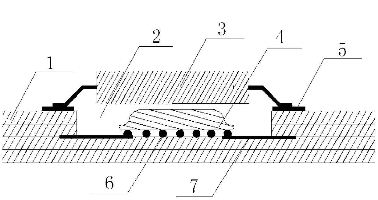
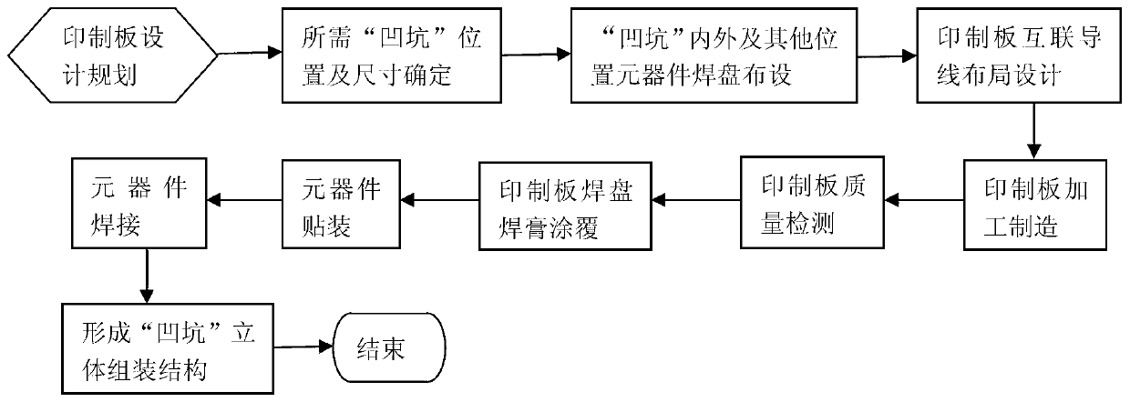
[0018] refer to figure 1 . According to the present invention, in a preferred embodiment described below, the cavity-embedded circuit substrate three-dimensional assembly structure first plans, designs and manufactures the sunken cavity 2 for assembling components on the printed board. During the manufacturing process of the printed board 1 , the depressed pits 2 are formed by controlling the shape of each layer of the printed board 1 . Then, according to the circuit principle design, the wiring design in the printed board 1 is carried out to complete the layout of the electrical signal transmission channels between the devices; a suitable jumper device 3 is arranged directly above the assembled device 4 in the sunken pit 2, for example, on the printed board 1 The layout above the sunken pit 2 is designed for devices with surrounding leads such as plastic-encapsulated lead chip carrier PLCC, square flat no-lead package QFN, and the like. Layout the selected thin and small c...


PUM


Abstract

The invention provides a pit embedded circuit board three-dimensional assembling method, which has the advantages of being capable of obviously improving the three-dimensional assembling density of electronic products, reducing the size and the weight and realizing time sequence consistency of transmitting signals of paired used devices. The invention is realized in the following technical scheme that sunken pits for assembling components are designed and manufactured on a printed board, and the selected thin and small components are deployed in the sunken pits of the printed board; appropriate bridging devices are deployed right above the pits to form a pit-type device lamination three-dimensional assembled structural form; wiring in the printed board is carried out according to the circuit design, electrical signal transmission channels are laid among the devices, and are connected with the devices inside and outside the sunken parts through printed conductors on the printed board; patching is carried out on the components on the surface of the printed board (comprising the surfaces of the pits), and device bonding pads are arranged inside and outside the sunken pits and solder paste is coated on the bonding pads according to the device bonding pad design; and the printed board plastered with the components is subjected to reflow soldering, thereby finishing the three-dimensional assembling of the printed board.

Description

technical field [0001] The invention relates to the board-level three-dimensional assembly structure form of electronic devices. Background technique [0002] In the 1990s, due to the development of ultra-large-scale and system-on-chip ICs, the development of peripheral pins to area array pins and ball grid array dense packaging was promoted, and it became the mainstream. Passive devices have developed to surface mount components (SMC), and continue to develop towards miniaturization. The packaging of IC devices has surface mount devices (SMD). During this period, SMD has developed greatly, resulting in ball grid Array package BGA, chip size package CSP, high-density high-performance low-cost FlipChip, multi-chip component MCM and other packaging forms, the assembly technology is SMT surface mount technology and reflow soldering, wave soldering, and continue to narrow pitch and ultra-narrow pitch SMT develop. All of these lead to more advanced packaging technology, the rat...

Claims


Application Information

Patent Timeline
IPC IPC(8): H05K3/34
Inventor 郑国洪郑大安
Owner 10TH RES INST OF CETC
Why Eureka
Try Eureka