

Silver-alloy sputtering target for conductive-film formation, and method for producing same
A technology of conductive film and manufacturing method, which is applied in semiconductor/solid-state device manufacturing, metal rolling, sputtering coating, etc., can solve problems such as short-circuit failure, migration, etc. Effect
- Summary
- Abstract
- Description
- Claims
- Application Information
AI Technical Summary
Problems solved by technology
Method used
Image

Examples
Embodiment 1)
[0084] Ag with a purity of 99.99% by mass or more and In as an additive raw material with a purity of 99.9% by mass or more were prepared and filled in a high-frequency induction melting furnace built with a black lead crucible. The total mass at the time of melting was set at about 1100 kg.
[0085] At the time of smelting, Ag was first smelted, and after Ag was melted, raw materials were added so that the target composition shown in Table 1 was obtained. The alloy molten metal is thoroughly stirred by the stirring effect of induction heating, and then cast in a cast iron mold.
[0086] The shrinkage cavity portion of the ingot obtained by this casting was cut off, and the surface in contact with the mold was removed by surface shaving, so that a rectangular parallelepiped ingot with an approximate size of 640×640×180 (mm) was obtained as a complete part.
[0087] This ingot was heated to 770° C., and rolling was repeated in one direction to extend from 640 mm to 1700 mm. T...
Embodiment 2~10、 comparative example 1~10)
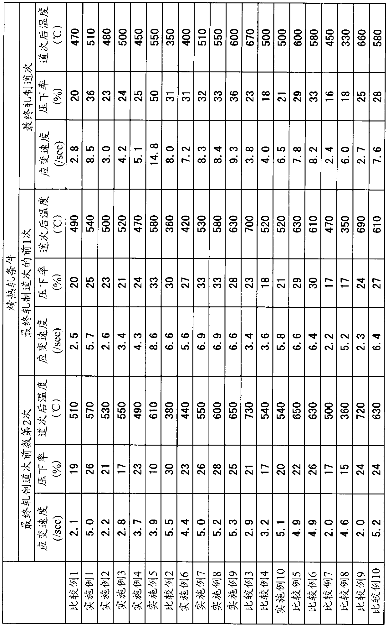
[0092] Same as in Example 1, changing within the following ranges: the heating temperature of the ingot before hot rolling is 510-880°C, the temperature of the plate after final rolling is 9.0-24.2mm, and the total number of passes is 10-14 times, and make the total rolling rate 87 to 95%. In addition, targets were prepared from the target composition shown in Table 3, the conditions from the last pass to the penultimate pass shown in Table 1, and the conditions of the cooling rate after hot rolling shown in Table 3. The cooling rate described in Table 3 means the cooling by water spray, and the "anhydrous cooling" means only standing cooling. However, the thickness of the target after machining shall be within the range of 6 to 21 mm.
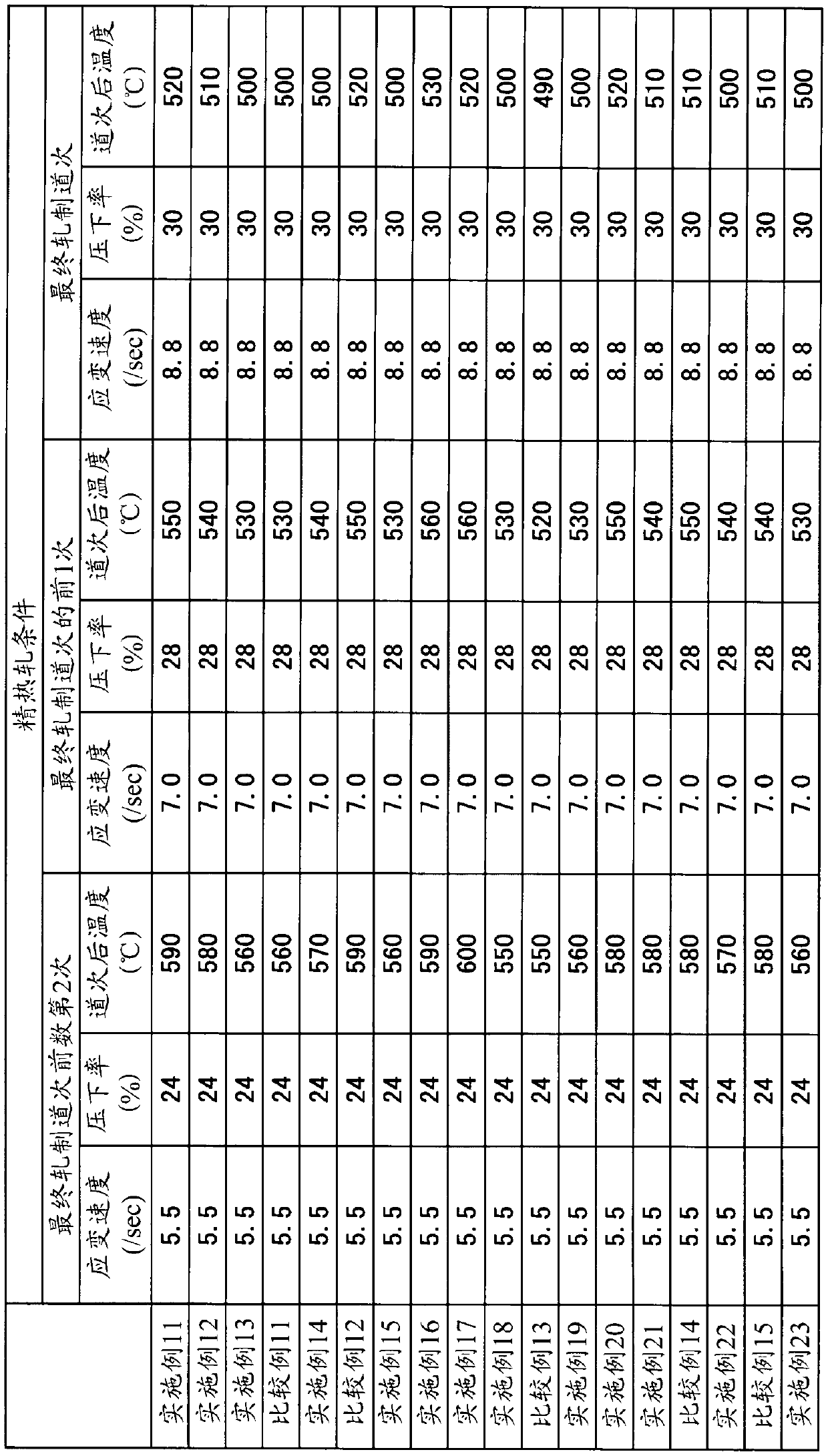
Embodiment 11~13、 comparative example 11)
[0094] Melting and casting were carried out in the same manner as in Example 1 to produce an ingot with an approximate size of 640×640×60 (mm). This ingot was heated to 700° C., followed by hot rolling to obtain a plate material with an approximate size of 1200×1300×16 (mm).
[0095] A total of 6 passes were repeated in this hot rolling. Among them, the conditions from the final pass to the penultimate third pass (strain rate per pass, reduction rate, sheet temperature after the pass) were set as in Table 2. The total rolling ratio of the whole hot rolling was 73%.
[0096] After the hot rolling, the rolled plate was quenched under the conditions shown in Table 3.
[0097] After cooling, the plate was passed through a roll leveler to correct the strain caused by quenching, and machined to a size of 1000×1200×12 (mm) as a target.
PUM
| Property | Measurement | Unit |
|---|---|---|
| particle size | aaaaa | aaaaa |
| particle size | aaaaa | aaaaa |
| thickness | aaaaa | aaaaa |
Abstract
Description
Claims
Application Information