

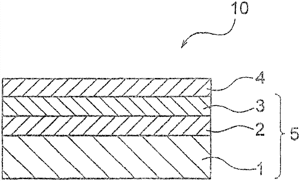
Film for laminating transparent conductive coatings, method of producing the same, and transparent conductive film
A technology of transparent conductive film and transparent substrate, applied in conductive layers on insulating carriers, chemical instruments and methods, lamination and other directions, can solve the problems of insufficient and difficult to identify lattice patterns, etc., and achieve the effect of high transmittance
- Summary
- Abstract
- Description
- Claims
- Application Information
AI Technical Summary
Problems solved by technology
Method used
Image

Examples
Embodiment
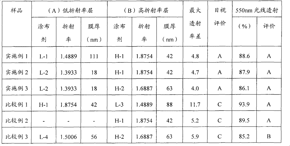
[0123] Next, although an Example demonstrates this invention in detail, this invention is not limited by these examples.
[0124] In addition, the refractive index was measured using the refractometer made by ATAGO company according to the A method of JISK7142:2008. In addition, the film thickness of (A) low-refractive-index layer and (B) high-refractive-index layer was measured using the ellipsometer.
[0125] Moreover, the following evaluation was performed about the electroconductive film obtained in each example.
[0126] (1) poor transmittance
[0127] The transmittance spectrum was measured on the laminated portion and non-laminated portion of (C) transparent conductive film of the produced transparent conductive film, and the maximum value of the absolute value of the transmittance difference in the wavelength range of 450 to 650 nm was obtained.
[0128] As a transmittance measuring instrument, a product model "UV-3600" manufactured by Shimadzu Corporation was used. ...
preparation example L-3
[0145] Preparation Example L-3 Coating Agent 3 for Low Refractive Index Layer
[0146]Except for using 4000 parts by mass of methyl isobutyl ketone and 4000 parts by mass of cyclohexanone as the dilution solvent, it was prepared in the same manner as in Preparation Example L-1, and a low refractive index layer with a solid content concentration of about 3.4 mass % was produced. Use coating agent L-3.
[0147] Preparation Example L-4 Coating Agent 4 for Low Refractive Index Layer
[0148] In addition to using 330 parts by mass of silica sol (manufactured by Nissan Chemical Co., Ltd., trade name "PGM-ST", 30 mass% of silica fine particles with an average particle diameter of 15nm, 70 mass% of propylene glycol monomethyl ether), 4750 mass 4,750 parts by mass of methyl isobutyl ketone, except that 4750 parts by mass of cyclohexanone was used as a diluting solvent, prepared in the same manner as in Preparation Example L-1, and a coating agent for a low-refractive index layer with ...
preparation example H-2
[0151] Preparation Example H-2 Coating Agent 2 for High Refractive Index Layer
[0152] As an active energy ray-curable compound, add 100 parts by mass of a hard coat agent (manufactured by Dainichi Seika Co., Ltd., trade name "SEIKABEAMXF-01L (NS)", with a solid content concentration of 100 mass%, containing a polyfunctional acrylate Active energy ray-curable compound 95% by mass, photopolymerization initiator 5% by mass) and 455 parts by mass of titanium oxide slurry (manufactured by Tayca Co., Ltd., 33% by mass of titanium oxide particles with an average particle diameter of 10 nm, propylene glycol monomethyl ether 67% by mass), 0.3 parts by mass of photopolymerization initiator (manufactured by BASF Corporation, trade name "Irgacure907", solid content concentration 100% by mass), as a dilution solvent, add 3000 parts by mass of methyl isobutyl ketone, 3000 parts by mass Parts of cyclohexanone were uniformly mixed to prepare a high-refractive index layer coating agent H-2 h...
PUM
| Property | Measurement | Unit |
|---|---|---|
| Film thickness | aaaaa | aaaaa |
| Film thickness | aaaaa | aaaaa |
Abstract
Description
Claims
Application Information