Transistor formation method and CMOS formation method

A technology of transistors and semiconductors, applied in semiconductor/solid-state device manufacturing, electrical components, circuits, etc., can solve the problems of small increase in carrier mobility, limited improvement in transistor performance, limited stress, etc., and achieve carrier mobility Increase, increase stress, performance improvement effect

Active Publication Date: 2013-09-18
SEMICON MFG INT (SHANGHAI) CORP
View PDF4 Cites 17 Cited by
  • Summary
  • Abstract
  • Description
  • Claims
  • Application Information

AI Technical Summary

Problems solved by technology

[0011] However, the transistor with the stress liner layer formed by the prior art provides limited stress to the channel region, and the impr

Method used


Image

  • Transistor formation method and CMOS formation method
  • Transistor formation method and CMOS formation method
  • Transistor formation method and CMOS formation method

Examples


Embodiment Construction

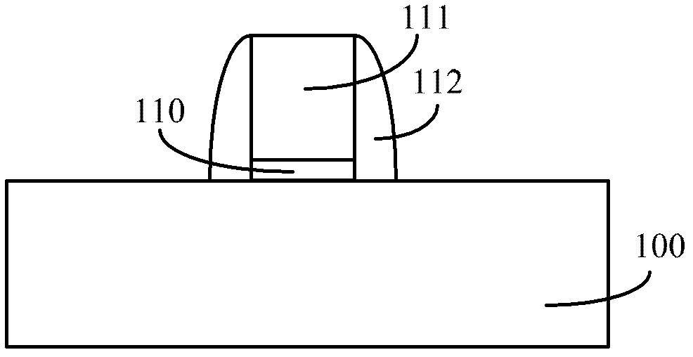
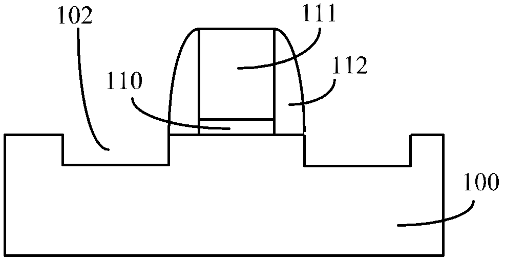
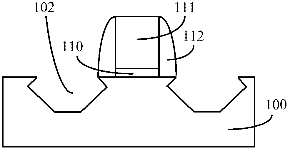
[0070] As mentioned in the background art, the transistor with the stress liner layer formed by the prior art provides limited stress to the channel region, and the improvement of the carrier mobility of the channel region is small, resulting in the formation of the transistor. Performance improvements are limited.

[0071] After research, the inventors found that the reason why the mobility of the transistor with the stress liner layer formed by the prior art is small is that in the existing method of forming the transistor with the stress liner layer, there will be Dry etching and wet etching are carried out in the semiconductor substrates on both sides to form sigma-shaped openings, so that the sidewalls in the gate structure are thinned during the dry etching and wet etching processes; Thin sidewalls easily transfer the stress formed by the stress liner layer to the sidewalls, so the stress obtained in the channel region is reduced, resulting in an insignificant increase i...


PUM

PropertyMeasurementUnit
Thicknessaaaaaaaaaa
Thicknessaaaaaaaaaa

Abstract

Provided are a transistor formation method and a CMOS formation method. The transistor formation method comprises: providing a semiconductor substrate which is formed with a gate dielectric layer, a gate electrode layer and a hard mask layer on the surface in sequence, wherein the two sides of the gate dielectric layer, the gate electrode layer and the hard mask layer are formed with first side walls and pseudo side walls in sequence; forming stress liner layers in the semiconductor substrate which is closely next to the two sides of the pseudo side walls; removing the pseudo side walls after the stress liner layers are formed and then forming second side walls on the outside surfaces of the first side walls; performing ion implantation on the stress liner layers after the second side walls are formed and then forming self-aligned silicide layers in the stress liner layers, wherein the surfaces of the self-aligned silicide layers are flush with the surfaces of the stress liner layers; and removing the hard mask layer after the self-aligned silicide layers are formed. With the transistor formation method, mobility of carriers in channel region is enhanced and performance of the transistor is improved.

Description

technical field [0001] The invention relates to the technical field of semiconductor manufacturing, in particular to a method for forming a transistor and a method for forming a CMOS. Background technique [0002] With the rapid development of semiconductor manufacturing technology, semiconductor devices are developing toward higher component density and higher integration in order to achieve higher computing speed, larger data storage capacity, and more functions. Therefore, gates of complementary metal oxide semiconductor (CMOS) transistors are becoming thinner and shorter than before. However, the size change of the gate will affect the electrical performance of semiconductor devices. At present, the performance of semiconductor devices is mainly improved by controlling the carrier mobility. A key element of the technology is controlling the stress in the transistor channel. For example, by properly controlling the stress and increasing the mobility of carriers (electro...

Claims


Application Information

Patent Timeline
IPC IPC(8): H01L21/8238
Inventor 李凤莲倪景华
Owner SEMICON MFG INT (SHANGHAI) CORP
Why Eureka
Try Eureka