Forming method of metallic oxide layer in resistive random access memory

A technology of resistive memory and oxide layer, which is applied in the direction of electrical components, etc., can solve the problems that the oxide layer cannot provide a high-quality oxide layer that meets the requirements, and the resistance change performance of the metal oxide layer is greatly affected, so as to improve the quality of the oxide layer, Good uniformity and high oxygen content

Active Publication Date: 2013-09-25
北京新忆科技有限公司
View PDF4 Cites 3 Cited by
  • Summary
  • Abstract
  • Description
  • Claims
  • Application Information

AI Technical Summary

Problems solved by technology

Among them, the oxygen content and other characteristics of the metal oxide layer have a great influence on the resistive switching performance.

Method used


Image

  • Forming method of metallic oxide layer in resistive random access memory
  • Forming method of metallic oxide layer in resistive random access memory

Examples


specific Embodiment

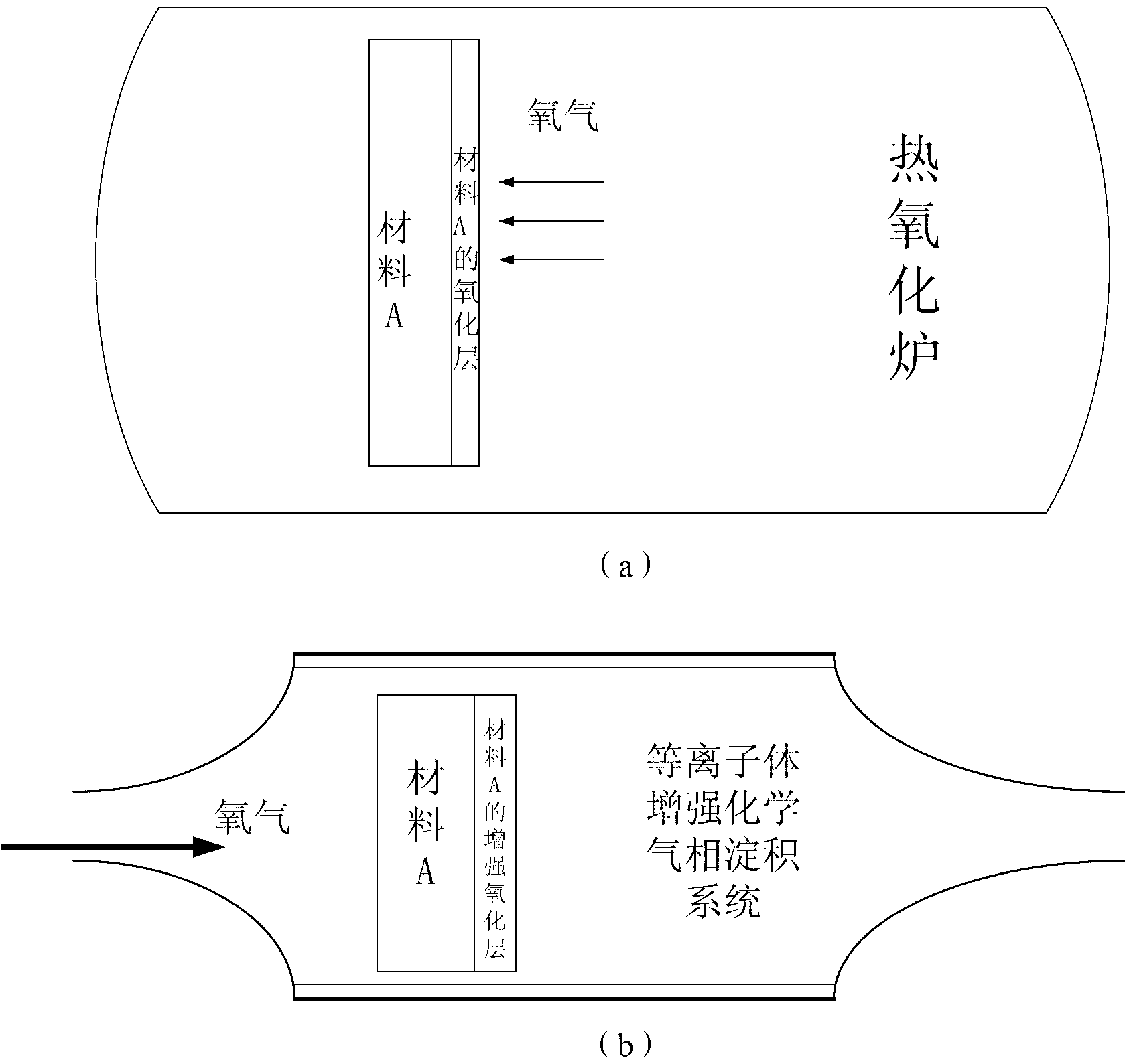
[0026] To enable those skilled in the art to better understand the present invention, the following is combined figure 2 Describe a specific example as follows:

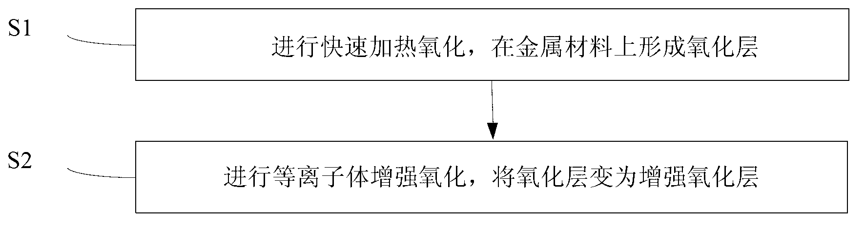
[0027] Such as figure 2 Shown is a schematic diagram of the step-by-step process of the present invention. The first step is the traditional thermal oxidation process. Dry oxygen oxidation of material A is carried out in a thermal oxidation furnace (horizontal / vertical oxidation system). The temperature for rapid heating and oxidation is 400-500℃, 50-200s, according to The oxide layer thickness required by the device design adjusts the process parameters to a certain extent. The common oxide layer thickness is 30-100nm. In the second step, the material is put into the plasma enhanced chemical vapor deposition system (including cold wall parallel plate / hot wall parallel plate / electron cyclotron resonance, etc.), oxygen is introduced to create an oxygen atmosphere, and plasma enhanced chemical vapor deposition is use...


PUM

PropertyMeasurementUnit
Thicknessaaaaaaaaaa

Abstract

The invention provides a forming method of a metallic oxide layer in a resistive random access memory. The forming method comprises the steps of carrying out fast heating oxidation to form an oxidation layer on a metal material and carrying out plasma body enhancing oxidation to change the oxidation layer to an enhancement oxidation layer. The metallic oxide layer manufactured through the method is high in oxygen content and good in uniformity.

Description

Technical field [0001] The invention relates to the field of semiconductor manufacturing, in particular to a method for forming a metal oxide layer in a resistive random access memory. Background technique [0002] With the gradual development of human science and technology, especially electronic devices and electronic products occupy more and more positions in human social life, the semiconductor market is still prospering despite the overall weakness of the world economy. Semiconductor technology drives the continuous progress of the electronics industry, which in turn promotes the development of the entire society. With the continuous development of semiconductor technology and the further popularization of electronic equipment in society, especially the popularization of portable electronics such as mobile phones and the development of special electronic equipment such as medical instruments, the size of microelectronics is constantly shrinking. Semiconductor process refers...

Claims


Application Information

Patent Timeline
IPC IPC(8): H01L45/00
Inventor 吴华强白越吴明昊钱鹤
Owner 北京新忆科技有限公司
Why Eureka
Try Eureka