III-nitride-based device structure containing multi-layer back-barrier

A device structure and back barrier technology, applied in the direction of semiconductor devices, electrical components, circuits, etc., can solve the problems of increasing the leakage of the buffer layer, the effect of the breakdown voltage is limited, and the composition is not too high, so as to improve the breakdown voltage, The effect of increasing the withstand voltage of the device

Active Publication Date: 2013-10-02
THE 13TH RES INST OF CHINA ELECTRONICS TECH GRP CORP
View PDF4 Cites 7 Cited by
  • Summary
  • Abstract
  • Description
  • Claims
  • Application Information

AI Technical Summary

Problems solved by technology

[0005] The effect of the single-layer back barrier structure on improving the breakdown voltage is limited. Firstly, the composition of the back barrier should not be too high, otherwise high concentration of two-dimensional hole gas (2DHG) will be introduced, which will increase the leakage of the buffer layer and the breakdown voltage. On the contrary, it decreases; but the effect of low back barrier composition on increasing channel confinement is very limited

Method used


Image

  • III-nitride-based device structure containing multi-layer back-barrier
  • III-nitride-based device structure containing multi-layer back-barrier
  • III-nitride-based device structure containing multi-layer back-barrier

Examples


Embodiment 1

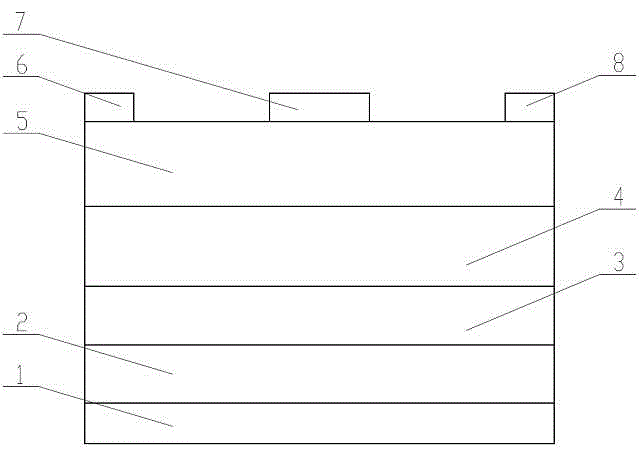
[0020] Depend on figure 1 It can be seen that Embodiment 1 is a multi-layer back barrier high electron mobility transistor HEMT based on Group III nitride materials, including a substrate layer 1, a back barrier structure layer, a channel layer 4 and a barrier layer from bottom to top 5. A source metal 6 , a gate metal 7 and a drain metal 8 are arranged on the barrier layer 5 . The back potential barrier structure layer is made up of the first back potential barrier 2 and the second back potential barrier 3, and the first back potential barrier 2 and the second back potential barrier 3 are Al x GaN (0

[0021] The substrate layer 1 is Si or sapphire; the channel layer 4 is GaN or Al x Ga 1-x N (0x al y Ga 1-x-y N (0≤x≤1, 0≤y≤1, x+y≤1).

[0022] The Al composition of the back barrier structure layer gradually increases linearly along the direction from the channel layer 4 to the substrate layer 1, that i...

Embodiment 2

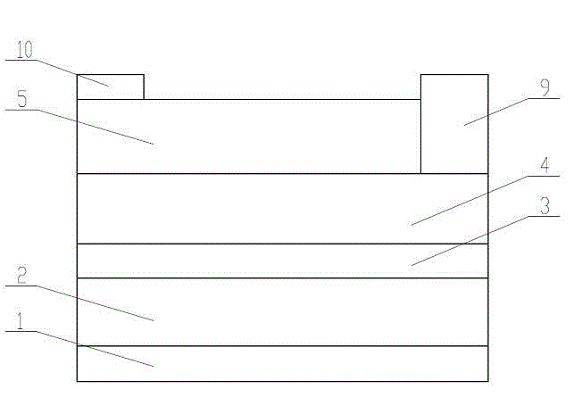
[0025] Depend on figure 2 It can be seen that Embodiment 2 is a multilayer back barrier Schottky diode SBD based on III-nitride materials, including a substrate layer 1, a back barrier structure layer, a channel layer 4 and a barrier layer 5 from bottom to top , an anode metal 10 is provided on the barrier layer 5 , and a cathode metal 9 is provided on the channel layer 4 . The back barrier structure layer is composed of a first back barrier 2 and a second back barrier 3 . The first back potential barrier 2 and the second back potential barrier 3 are Al x GaN (0

[0026] The substrate 1 is SiC or GaN or diamond; the channel layer 4 is GaN; the barrier layer 5 is In x al y Ga 1-x-y N (0≤x≤1, 0≤y≤1, x+y≤1).

[0027] The Al composition of the back barrier structure layer gradually increases nonlinearly along the direction from the channel layer 4 to the substrate layer 1 . That is, the Al composition of ...

Embodiment 3

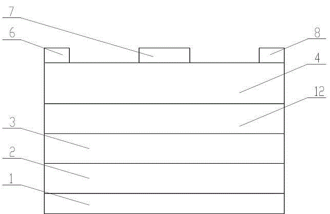
[0030] Depend on image 3 It can be seen that Embodiment 3 is a multi-layer back barrier Schottky barrier field effect transistor MESFET based on Group III nitride materials, including a substrate layer 1, a back barrier structure layer, and a channel layer 4 from bottom to top. A source metal 6 , a gate metal 7 and a drain metal 8 are disposed on the channel layer 4 . The back potential barrier structure layer is made up of the first back potential barrier 2, the second back potential barrier 3 and the third back potential barrier 12, the first back potential barrier 2, the second back potential barrier 3 and the third back potential barrier 12 for Al x GaN (0

[0031] The substrate layer 1 is Si or sapphire or SiC or GaN or diamond; the channel layer 4 is GaN or Al x Ga 1-x N (0

[0032] The Al composition of the back barrier structure layer gradually increases nonlinearly along the direction fro...


PUM


Abstract

The invention discloses an III-nitride-based device structure containing multi-layer back-barrier, which belongs to the field of semiconductor devices. The device structure comprises a substrate layer, a back-barrier structure layer and a channel layer from the top down, wherein the back-barrier structure layer is composed of two or more back-barriers of AlxGaN (0<x<1) with different Al components; the Al component increases gradually from the channel layer to the substrate layer, and remains unchanged within the same back-barrier layer. The back-barrier structure layer reduces channel electric field peak value, effectively regulates the channel electric field, and increases the breakdown voltage of the device; compared with the field plate technology, the multi-layer back-barrier structure does not increase the gate capacitance, thereby having a small influence of frequency characteristic of the device; compared with single-layer back-barrier structure, the multi-layer back-barrier structure can use multi-layer low-component back-barriers to regulate the channel electric field together without introducing 2DHG (two-dimensional hole gas), so as to effectively increase device voltage withstanding on the basis of a higher device saturation current.

Description

technical field [0001] The present invention relates to the field of semiconductor devices. Background technique [0002] GaN semiconductor material has excellent properties such as larger forbidden band width, higher critical breakdown electric field and electron saturation drift speed, and has attracted extensive attention of researchers. Although the critical breakdown electric field of GaN material is much higher than that of other semiconductor materials, due to the local curvature effect of GaN devices, there is a peak electric field inside the device, which makes the device breakdown in advance. Therefore, how to reduce the peak electric field, alleviate the local curvature effect, and improve the breakdown voltage of devices has always been one of the research hotspots at home and abroad. [0003] Field plate technology is the simplest and most effective way to improve the withstand voltage of devices. The Mishra group reported the world's first high-voltage power ...

Claims


Application Information

Patent Timeline
Patent Type & Authority Applications(China)
IPC IPC(8): H01L29/778H01L29/872H01L29/06
Inventor 王元刚冯志红敦少博吕元杰房玉龙徐鹏
Owner THE 13TH RES INST OF CHINA ELECTRONICS TECH GRP CORP
Why Eureka
Try Eureka