

A silicon solar cell with a thin film covering the front electrode and its manufacturing process
一种太阳能电池、制造工艺的技术,应用在太阳能电池领域,能够解决影响电池转换效率、易被腐蚀和氧化、接触面积减少等问题,达到提高电池转换效率、提高抗腐蚀性和抗氧化能力、降低串联电阻的效果
- Summary
- Abstract
- Description
- Claims
- Application Information
AI Technical Summary
Problems solved by technology
Method used
Image

Examples
Embodiment 1
[0044] Embodiment 1: This embodiment provides a manufacturing process of thin-film covered MWT solar cells, which is completed through the following process steps:
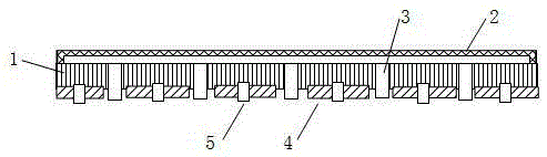
[0045] 1) Punching: Use a laser to open a through hole 1 with a diameter of 200-300 microns at a predetermined position on the selected P-type silicon wafer. The so-called predetermined position is the position of the front electrode 3 of the solar cell, and the number of through holes is also the same as that of the front electrode 3. The number is the same.
[0046] 2) Texturing: Use HF and HNO3 to corrode the silicon wafer, forming a 1-3 micron egg structure on the surface of the silicon wafer.
[0047] 3) Diffusion: Phosphorus oxychloride and oxygen are used to diffuse phosphorus on the silicon wafer at high temperature. The diffusion resistance is 85 ohms to form a PN junction.
[0048] 4) Through hole back junction protection: A paraffin mask is printed on the back of the solar cell through hole to protect the throu...
Embodiment 2
[0056] Embodiment 2: This embodiment proposes a thin film covering MWT structure SE solar cell manufacturing process, including the following steps:
[0057] 1) Punching: Use a laser to open a through hole 1 with a diameter of 200-300 microns at a predetermined position on the selected P-type silicon wafer. The so-called predetermined position is the position of the front electrode 3 of the solar cell, and the number of through holes is also the same as that of the front electrode 3. The number is the same.
[0058] 2) Texturing: Use HF and HNO3 to corrode the silicon wafer, forming a 1-3 micron egg structure on the surface of the silicon wafer.
[0059] 3) Diffusion: Phosphorus oxychloride and oxygen are used to diffuse phosphorus on the silicon wafer at high temperature. The diffusion resistance is 85 ohms to form a PN junction.
[0060] 4) Through hole back junction protection: A paraffin mask is printed on the back of the solar cell through hole to protect the through hole and the...
PUM
 Abstract
Description
Claims
Application Information