Pd-coated copper ball bonding wire

A coating, copper wire technology, applied in conductive materials, conductors, electrical components, etc., can solve problems such as peeling and bonding interfaces, and achieve the effect of reliable stabilization and excellent high temperature stability

Active Publication Date: 2013-10-02
TANAKA DENSHI KOGYO KK
View PDF11 Cites 20 Cited by
  • Summary
  • Abstract
  • Description
  • Claims
  • Application Information

AI Technical Summary

Problems solved by technology

[0006] However, in the case of using these copper wires for semiconductor applications placed in a high-temperature environment of 80°C to 200°C, even if ball bonding can be smo

Method used


Image

  • Pd-coated copper ball bonding wire
  • Pd-coated copper ball bonding wire
  • Pd-coated copper ball bonding wire

Examples


Embodiment 1

[0071] Examples are described below.

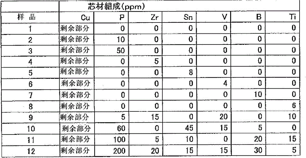
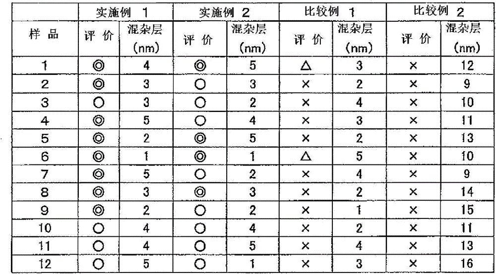
[0072] A copper wire drawn from a copper (Cu) ingot described in Table 1 to a wire diameter of 500 μm was used as a core material, and an electrolytic plating film of a 2.0 μm palladium (Pd) intermediate layer was deposited on the surface of the wire by a usual method. The palladium (Pd) plating bath was obtained by adding 10 gW / l of phosphate to a neutral dinitrodiamine palladium bath, and the purity of the obtained palladium (Pd) was 99%. Next, gold (Au) with a purity of 99.99% by mass was magnetron sputtered at room temperature to deposit 0.08 μm. In addition, the coating thickness was measured by Auger electron spectroscopy (AES).

[0073] Thereafter, the coated copper wire was die-drawn to a final diameter of 17 μm. The theoretical film thickness of gold (Au) is 0.0027 μm. Next, processing strain is removed, and a predetermined final heat treatment is performed until the elongation value reaches about 10%. As for the final ...

Embodiment 2

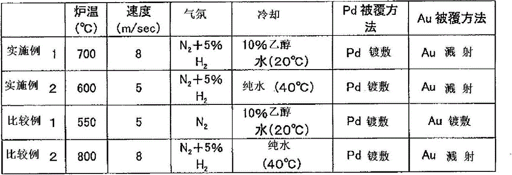
[0078] The coated copper wire produced under the same conditions as in Example 1 was passed through a heat treatment furnace at 600° C. in a 5% hydrogen+nitrogen atmosphere at a speed of 5 m / s, and cooled in pure water (40° C.).


PUM

PropertyMeasurementUnit
Wire diameteraaaaaaaaaa
The average thicknessaaaaaaaaaa

Abstract

To increase the reliability of joins to an aluminum electrode in a palladium-coated copper wire for ball bonding, a gold (Au) layer comprising an ultra-thin layer having a thickness of no greater than 5 nm is formed at the surface of a palladium (Pd) intermediate layer and heat processing is performed in an inert atmosphere containing hydrogen, causing the palladium of the intermediate layer to infiltrate the ultra-thin gold layer, forming a gold-palladium intermingled layer by means of Stranski-Krastanov growth such that a minute gold phase and palladium phase grow in 3D. In the heat processing process, the palladium absorbs hydrogen, and by means of rapid cooling after heat processing, the palladium in the intermingled layer is stabilized, and along with the gold that melts early during molten ball formation and covers a wire end surface, the palladium that has reached the end surface melts and is dispersed uniformly and minutely at the molten ball surface layer, suppressing the oxidation of aluminum at the bond interface with the aluminum.

Description

technical field [0001] The present invention relates to a Pd-coated copper wire for connecting electrodes on a semiconductor element and wiring on a circuit wiring board by ball bonding. Background technique [0002] At present, gold wires having a wire diameter of about 15 to 30 μm are mainly used as bonding wires for bonding electrodes on semiconductor elements and external terminals by ball bonding. However, with the rise in the price of gold ingots in recent years, instead of the current high-purity 4N-based (99.99% by mass or higher) gold wires, copper wires with a wire diameter of about 10 to 25 μm have attracted attention. [0003] It is considered that the copper wire can be used in the same application field as the gold wire. For example, in the mounting relationship, in addition to the current QFP (Quad Flat Packaging) using the lead frame, substrates and polyimide tapes are also used. The application of new forms such as BGA (Ball Grid Array) and CSP (Chip Scale ...

Claims


Application Information

Patent Timeline
IPC IPC(8): H01L21/60
CPCH01B1/026H01L24/05H01L24/43H01L24/45H01L2224/04042H01L2224/05624H01L2224/43H01L2224/4321H01L2224/45015H01L2224/45144H01L2224/45147H01L2224/45572H01L2224/45573H01L2224/45644H01L2224/45655H01L2224/45664H01L2224/45669H01L2224/48227H01L2224/48247H01L2224/48463H01L2224/48465H01L2224/48624H01L2224/48639H01L2224/48644H01L2224/48655H01L2224/48664H01L2224/48824H01L2224/48839H01L2224/48844H01L2224/48855H01L2224/48864H01L2224/85181H01L2224/85439H01L2224/85444H01L2224/85455H01L2224/85464H01L2924/00011H01L2924/01006H01L2924/01015H01L2924/01047H01L2924/10252H01L2924/10253H01L2924/12041H01L2924/181H01L2924/01202H01L2924/01203H01L2924/20751H01L2924/20752H01L2924/00015H01L2924/00H01L2924/01008H01L2924/013H01L2924/00014H01L2924/01029H01L2924/00013H01L2924/01028H01L2924/01027H01L2924/01204H01L2924/01205H01L2924/01206H01L2924/0105H01L2924/0104H01L2924/01023H01L2924/01005H01L2924/01022H01L2924/01001H01L2224/45565H01L2924/01004H01L2924/01033
Inventor 高田满生山下勉执行裕之桑原岳冈崎纯一齐藤茂
Owner TANAKA DENSHI KOGYO KK
Why Eureka
Try Eureka