Method for forming semiconductor device and method for forming MIM capacitor

A semiconductor and capacitor technology, applied in semiconductor/solid-state device manufacturing, circuits, electrical components, etc., can solve problems such as poor reliability of MIM capacitors, and achieve good reliability, uniform thickness, and good electrical performance

Active Publication Date: 2013-10-09
SHANGHAI HUAHONG GRACE SEMICON MFG CORP
View PDF5 Cites 10 Cited by
  • Summary
  • Abstract
  • Description
  • Claims
  • Application Information

AI Technical Summary

Problems solved by technology

[0005] However, when detecting the MIM capacitor formed by the above process, it is found that the reliability of the formed MIM capacitor is poor

Method used


Image

  • Method for forming semiconductor device and method for forming MIM capacitor
  • Method for forming semiconductor device and method for forming MIM capacitor
  • Method for forming semiconductor device and method for forming MIM capacitor

Examples


Embodiment Construction

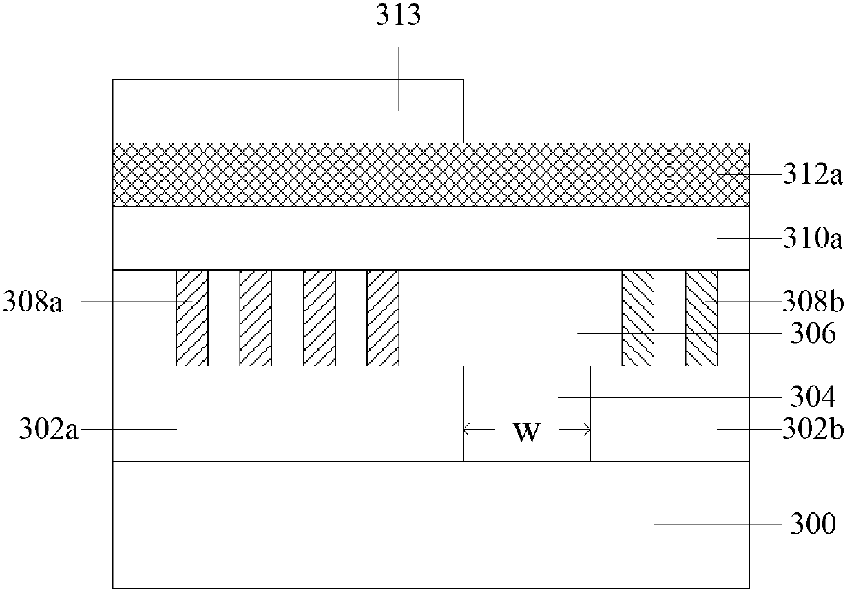
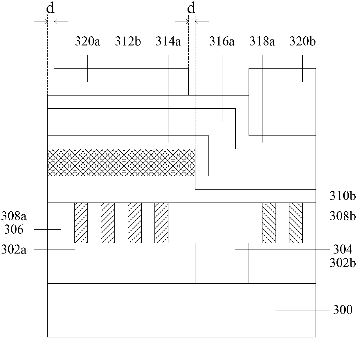
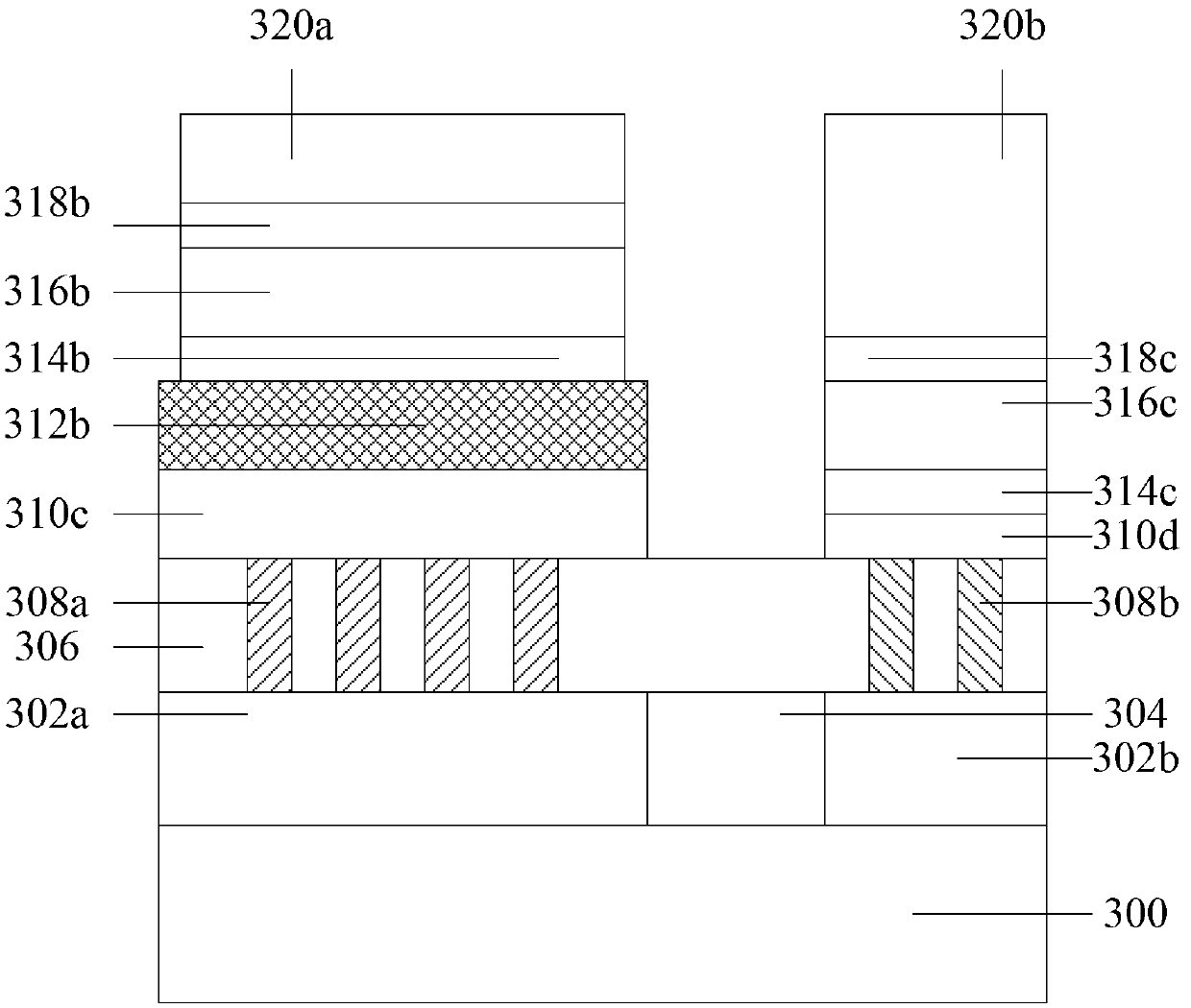
[0036] As mentioned in the background section, MIM capacitors formed by existing processes have poor reliability.

[0037] The reason for the poor reliability of existing MIM capacitors is that aluminum is a metal crystal, and the size of its crystal grains is uneven. The surface is uneven, which leads to the uneven lower surface of the subsequently formed capacitor dielectric layer; silicon oxide and silicon nitride are amorphous, and are formed on the capacitor dielectric layer made of silicon oxide or silicon nitride on the aluminum metal layer The surface is flat, and the upper and lower surfaces of the titanium nitride layer are flat, so the thickness of the capacitor dielectric layer located between the aluminum metal layer and the titanium nitride layer is not uniform. Since the breakdown voltage of the MIM capacitor is determined by the thinnest part of the capacitor dielectric layer, the breakdown voltage of the formed MIM capacitor changes greatly, and the MIM capaci...


PUM

PropertyMeasurementUnit
thicknessaaaaaaaaaa
thicknessaaaaaaaaaa
thicknessaaaaaaaaaa

Abstract

The invention provides a method for forming a semiconductor device and a method for forming an MIM capacitor. The method for forming the semiconductor device comprises the steps that a substrate is provided; a first interlayer dielectric layer which comprises a first metal interconnection layer and a second metal interconnection layer is formed on the substrate; a second interlayer dielectric layer which comprises first metal plugs and second metal plugs is formed on the first interlayer dielectric layer, the first metal interconnection layer and the second metal interconnection layer; a first conductive material layer is formed on the second interlayer dielectric layer, the first metal plug and the second metal plug; a capacitor dielectric layer is formed on the first conductive material layer above the first metal interconnection layer; a second conductive material layer is formed on the capacitor dielectric layer and the first conductive material layer; the second conductive material layer and the first conductive material layer above the first interlayer dielectric layer placed between the first metal interconnection layer and the second metal interconnection layer are etched until the second interlayer dielectric layer is exposed. The semiconductor device formed by the method is good in electrical property.

Description

technical field [0001] The invention relates to the field of semiconductor technology, in particular to a method for forming a semiconductor device and a method for forming an MIM capacitor. Background technique [0002] Passive devices such as resistors and capacitors are widely used in integrated circuit manufacturing technology. These devices usually use standard integrated circuit technology, using conductive materials such as doped single crystal silicon and doped polycrystalline silicon, and insulating films such as oxide films and nitrogen oxide films. material, such as PIP (poly-Insulator-Poly) capacitors. These devices are relatively close to the silicon substrate, and the parasitic capacitance between the device and the substrate will affect the performance of the device, especially in radio frequency (RF) circuits, as the frequency increases, the performance of the device decreases rapidly. [0003] The proposal of MIM (Metal-Insulator-Metal, metal-insulator-meta...

Claims


Application Information

Patent Timeline
Patent Type & Authority Applications(China)
IPC IPC(8): H01L21/02H01L21/768
Inventor 黎坡
Owner SHANGHAI HUAHONG GRACE SEMICON MFG CORP
Why Eureka
Try Eureka