Gallium nitride Schottky diode and manufacturing method thereof

A technology of Schottky diodes and manufacturing methods, applied in semiconductor/solid-state device manufacturing, electrical components, circuits, etc., can solve the problems of large reverse leakage, low withstand voltage and power, multi-wafer area, etc., and achieve reverse The effect of small leakage current, small turn-on voltage, high voltage and power

Active Publication Date: 2013-10-09
GPOWER SEMICON
View PDF3 Cites 24 Cited by
  • Summary
  • Abstract
  • Description
  • Claims
  • Application Information

AI Technical Summary

Problems solved by technology

[0004] figure 1 Shown is the MESA structure of a traditional GaN Schottky diode. The heavily doped n-type GaN and the lightly doped n-type GaN are sequentially deposited on the substrate, and the lightly doped n-type GaN is partially etched by mesa. The metal of the cathode and the heavily doped Dopant n-type GaN forms an Ohmic contact, and the metal of the anode forms a Schottky contact (Schottky contact) with lightly doped n-type GaN. This traditional GaN Schottky diode has good switching performance and high load voltage. The advantage, but the disadvantage is that the reverse leakage is relatively large, the reverse withstand voltage and power are relatively low, and the forward current density is relatively low due to the limitation of unipolar charges; at the same time, the planar structure will take up more Wafer area

Method used


Image

  • Gallium nitride Schottky diode and manufacturing method thereof
  • Gallium nitride Schottky diode and manufacturing method thereof
  • Gallium nitride Schottky diode and manufacturing method thereof

Examples


Embodiment Construction

[0040] The technical solutions in the embodiments of the present invention will be described in detail below in conjunction with the accompanying drawings in the embodiments of the present invention. Obviously, the described embodiments are only some of the embodiments of the present invention, not all of them. Based on the embodiments of the present invention, all other embodiments obtained by persons of ordinary skill in the art without making creative efforts belong to the protection scope of the present invention.

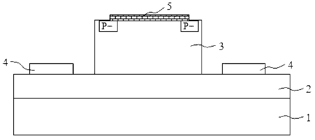
[0041] figure 1Shown is the traditional MESA structure of GaN Schottky diodes. On the substrate 1, heavily doped n-type GaN2 and lightly doped n-type GaN3 are sequentially deposited, and the lightly doped n-type GaN3 is partially etched by mesa. The metal of the cathode and the heavy Doped n-type GaN2 forms an ohmic contact 4, and the anode metal and lightly doped n-type GaN3 form a Schottky contact 5. This traditional GaN Schottky diode has the advantages of g...


PUM


Abstract

A manufacturing method of a GaN Schottky diode comprises the steps: providing a substrate; depositing a nucleating layer and / or a buffering layer on the substrate; depositing a heavy-doping n-type GaN layer on the nucleating layer and / or the buffering layer, and depositing a light-doping n-type GaN layer on the heavy-doping n-type GaN layer; arranging a plurality of p-type heavy-ion-doping GaN regions on the surface of the light-doping n-type GaN layer; depositing an insulation layer or a medium layer on the surface of the light-doping n-type GaN layer; defining a Schottky electrode region on the insulation layer, and trepanning the Schottky electrode region; depositing a Schottky electrode on the trepanned Schottky electrode region, wherein the Schottky electrode makes contact with the surface of the light-doping n-type GaN layer; defining an ohmic electrode region on the substrate, and trepanning the ohmic electrode region; depositing an ohmic electrode in the trepanned ohmic electrode region, wherein the ohmic electrode makes contact with the heavy-doping n-type GaN layer. The forward starting voltage of the Schottky diode is small, and a larger current can pass through in the forward direction; a leaked current in the backward direction is small, and larger voltage and power can be borne in the backward direction.

Description

technical field [0001] The invention relates to the technical field of semiconductor manufacturing, in particular to a gallium nitride Schottky diode and a manufacturing method thereof. Background technique [0002] With the development of the semiconductor industry, the performance of high-power semiconductor devices based on single crystal silicon has been difficult to meet the application requirements of various industries. The performance limit of silicon in the high-power field has promoted the large-scale development of high-power semiconductor devices based on gallium nitride (GaN, Gallium Nitride) in recent years. The third-generation semiconductor materials represented by gallium nitride have excellent characteristics, such as: large band gap, high breakdown electric field strength, high maximum current density, stable chemical properties, high thermal stability coefficient, small thermal expansion coefficient, etc. , is gradually replacing the application of silic...

Claims


Application Information

Patent Timeline
Patent Type & Authority Applications(China)
IPC IPC(8): H01L21/329H01L29/872H01L29/06
Inventor 宋晰
Owner GPOWER SEMICON
Why Eureka
Try Eureka