A production process for improving bipolar transistor bvcbo

A bipolar transistor and production process technology, applied in the field of electronics, can solve the problems of reducing the net doping concentration, limiting the increase and stability of the BVcbo breakdown voltage, and decreasing the radius of curvature of the junction terminal junction, so as to achieve high output power and increase the curvature. Radius, the effect of increasing the breakdown voltage

Active Publication Date: 2016-02-24
江苏博普电子科技有限责任公司
View PDF4 Cites 2 Cited by
  • Summary
  • Abstract
  • Description
  • Claims
  • Application Information

AI Technical Summary

Problems solved by technology

[0003] Although the NPN silicon bipolar microwave power transistor device manufactured by the above invention has increased the BVcbo breakdown voltage by more than 40%, due to the high temperature thermal process of field oxidation, the P-type dopant element boron implanted at the junction terminal tends to be absorbed (segregation) into the trench field oxide layer, while the N-type dopant elements arsenic or phosphorus in the epitaxial layer tend to be accumulated (segregation) in the silicon surface layer adjacent to the trench field oxide layer, so that in silicon at the silicon-silicon oxide interface (eg figure 1 As shown in 61) the P-type net doping concentration decreases, the radius of curvature of the junction terminal junction decreases, and is easily affected by the silicon-silicon oxide interface charge, which limits the further improvement and stability of the BVcbo breakdown voltage

Method used


Image

  • A production process for improving bipolar transistor bvcbo
  • A production process for improving bipolar transistor bvcbo
  • A production process for improving bipolar transistor bvcbo

Examples


Embodiment Construction

[0029] The present invention will be further described below in conjunction with the accompanying drawings.

[0030] The process flow of the above-mentioned NPN silicon bipolar microwave power transistor manufactured by the present invention is described in detail below as shown in the figure.

[0031] A kind of production technology that improves bipolar transistor BVcbo, comprises the steps:

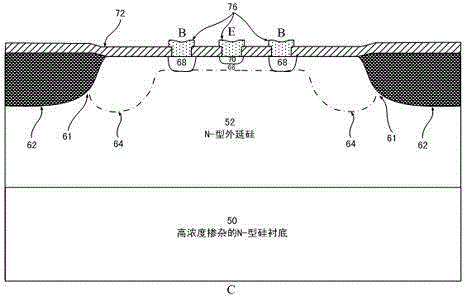
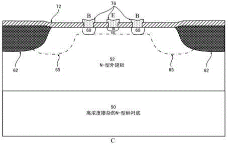
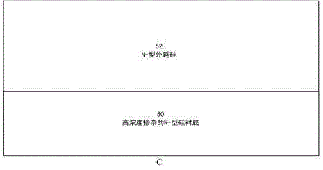
[0032] Step (1): Please refer to image 3, firstly, a highly doped N-type silicon substrate 50 is selected as the extrinsic collector region of the NPN transistor, and the back of the substrate 50 is thinned and gold evaporated after the transistor manufacturing process is completed for forming The collector C of the transistor; the crystal orientation of the substrate 50 can be or , but usually the crystal orientation is selected, and the doped impurity element can be arsenic (As) or It is phosphorus (P) or antimony (Sb), but it is usually arsenic, and the resistivity of the subst...


PUM


Abstract

The invention discloses a technology for improving bipolar transistor BVcbo production. The groove field oxide isolation process technology is combined with the junction terminal process technology, firstly, after a groove is formed through a dry etching process technology and before field oxidation of the groove is carried out, P-type element boron ions are pre-doped into groove field silicon through an ion implantation technology, then a field oxidation process of the groove is divided into two steps, and junction terminal boron ion implantation is arranged to be carried out between the two steps of field oxidation. According to a NPN silicon bipolar microwave power transistor device manufactured by using the process technology, not only is BVcbo breakdown voltage improved by more than 50%, but also high output power can be provided, stray capacitance of a collector junction is reduced, and high-frequency performance of the device is guaranteed.

Description

technical field [0001] The invention relates to a production process, in particular to a production process for improving a bipolar transistor BVcbo, and belongs to the field of electronic technology. Background technique [0002] High-frequency (RF and microwave) power transistor devices are widely used in communication systems and radar systems. The application design of microwave power transistor devices requires high output power and high gain. The operating frequency ranges from several hundred MHz to several GHz . In order to achieve such high output power, high gain and high frequency requirements, in addition to optimizing the layout of chip devices, selection of process parameters and packaging, it is sometimes more important to improve the manufacturing process of transistor chips. Based on this purpose, the invention of "a bipolar transistor with improved BVcbo and its production process", the patent application number: 2013102552435 gives a solution: by combinin...

Claims


Application Information

Patent Timeline
Patent Type & Authority Patents(China)
IPC IPC(8): H01L21/331H01L21/265
Inventor 陈强张复才沈美根多新中郑立荣姚荣伟
Owner 江苏博普电子科技有限责任公司
Why Eureka
Try Eureka