A multi-ceramic-layer patterned structure substrate for optical and electronic devices

A technology of electronic devices and ceramic layers, applied in the field of electronics, can solve problems such as difficult heat transfer, electrical conduction short circuit, etc., and achieve the effects of solving heat dissipation problems, good electrical isolation and thermal isolation, and high withstand voltage breakdown performance

A technology of electronic devices and ceramic layers, applied in the field of electronics, can solve problems such as difficult heat transfer, electrical conduction short circuit, etc., and achieve the effects of solving heat dissipation problems, good electrical isolation and thermal isolation, and high withstand voltage breakdown performance

CN103354221AActive Publication Date: 2013-10-16SUZHOU JINGPIN OPTOELECTRONICS

Image

  • A multi-ceramic-layer patterned structure substrate for optical and electronic devices
  • A multi-ceramic-layer patterned structure substrate for optical and electronic devices

Examples


Embodiment 1

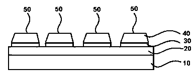
[0022] as attached figure 1 As shown, the multi-ceramic layer patterned structural substrate for optical and electronic devices described in this embodiment includes an aluminum or aluminum alloy substrate 10, and a SiC pressure-resistant ceramic layer 20 and AlN are sequentially formed on the metal substrate. High thermal conductivity ceramic layer 40; there is an aluminum transition layer 30 between the SiC pressure-resistant ceramic layer 20 and the AlN high thermal conductivity ceramic layer 40, and the AlN high thermal conductivity ceramic layer 40 and the aluminum transition layer 30 are selectively selected by a mask Etching forms a plurality of isolation pedestals 50; and forming a metal circuit layer (not shown in the figure) on the uppermost layer of the multi-ceramic layer of the isolation pedestals. The SiC pressure-resistant ceramic layer is prepared by an arc ion plating deposition method, with a thickness of 200 um. Wherein, the step of the aluminum transition ...

Embodiment 2

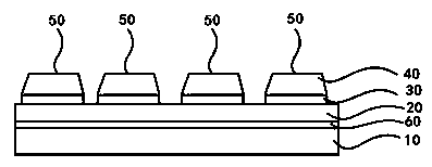
[0024] as attached figure 2 As shown, the multi-ceramic layer patterned structural substrate for optical and electronic devices described in this embodiment includes an aluminum or aluminum alloy substrate 10, and a SiC pressure-resistant ceramic layer 20 and AlN are sequentially formed on the metal substrate. High thermal conductivity ceramic layer 40; there is an aluminum transition layer 30 between the SiC pressure-resistant ceramic layer 20 and the AlN high thermal conductivity ceramic layer 40, and an active braze is arranged between the aluminum alloy substrate 10 and the SiC pressure-resistant ceramic layer 20 Welding layer 60; and selectively etch the AlN high thermal conductivity ceramic layer 40 and the aluminum transition layer 30 through a mask to form a plurality of isolation bases 50; and form on the uppermost layer of the multi-ceramic layer of the isolation base metal circuit layer (not shown in the figure). The SiC pressure-resistant ceramic layer is prepare...


PUM

PropertyMeasurementUnit
Thicknessaaaaaaaaaa
Thicknessaaaaaaaaaa

Abstract

The invention relates to a multi-ceramic-layer patterned structure substrate for optical and electronic devices. The multi-ceramic-layer patterned structure substrate comprises a metal substrate, wherein a voltage-withstanding ceramic layer and a high heat-conducting ceramic layer are sequentially formed on the metal substrate; a transition layer is arranged between the voltage-withstanding ceramic layer and the high heat-conducting ceramic layer; multiple isolation bases are formed by selective etching on the high heat-conducting ceramic layer and the transition layer through a mask; and a metal circuit layer is formed on every isolation base. The multi-ceramic-layer patterned structure substrate for optical and electronic devices has a metal substrate in a relatively large size, can accommodate multiple optical and / or electronic devices, and is provided with good electrical isolation and thermal isolation between the multiple optical and / or electronic devices.

Description

technical field [0001] The invention belongs to the field of electronic technology, and more specifically, the invention relates to a multi-ceramic layer patterned structural substrate for optical and electronic devices. Background technique [0002] Devices used in optics and / or electronics, such as integrated circuits or laser diodes, require the use of thermally conductive materials for heat transfer. For this purpose, a metallic base body is used, for example a copper base body, and an electrical isolation is often required between the optical and / or electronic components and the metal base body. And some ceramic materials have higher heat transfer efficiency and are electrically insulating. For this purpose, highly thermally conductive ceramic materials are frequently used as intermediate materials for providing electrical isolation while still maintaining thermal conductivity between the optical and / or electronic components and the metal base body. In order to provid...

Claims


Application Information

Patent Timeline
16 Oct 2013
Publication
CN103354221A
IPC
H01L23/14; H01L23/373
Inventors
高éž