A kind of unidirectional conductive withstand voltage device and its manufacturing method

A technology of unidirectional conduction and manufacturing method, which is applied in the manufacture of unidirectional conduction withstand voltage devices and the field of unidirectional conduction withstand voltage devices, which can solve the problems of small forward conduction current and increased resistance, and achieve high breakdown voltage resistance Effect

Active Publication Date: 2016-06-08
SHANGHAI HUAHONG GRACE SEMICON MFG CORP
View PDF5 Cites 0 Cited by
  • Summary
  • Abstract
  • Description
  • Claims
  • Application Information

AI Technical Summary

Problems solved by technology

The disadvantage of PN junction diodes is that the larger the reverse bias voltage is, the wider the required breakdown depletion layer width is, and at the same time, the resistance during forward turn-on increases accordingly. With the increase of the breakdown voltage of the device, the device can be obtained The forward conduction current is getting smaller and smaller

Method used


Image

  • A kind of unidirectional conductive withstand voltage device and its manufacturing method
  • A kind of unidirectional conductive withstand voltage device and its manufacturing method
  • A kind of unidirectional conductive withstand voltage device and its manufacturing method

Examples


Embodiment Construction

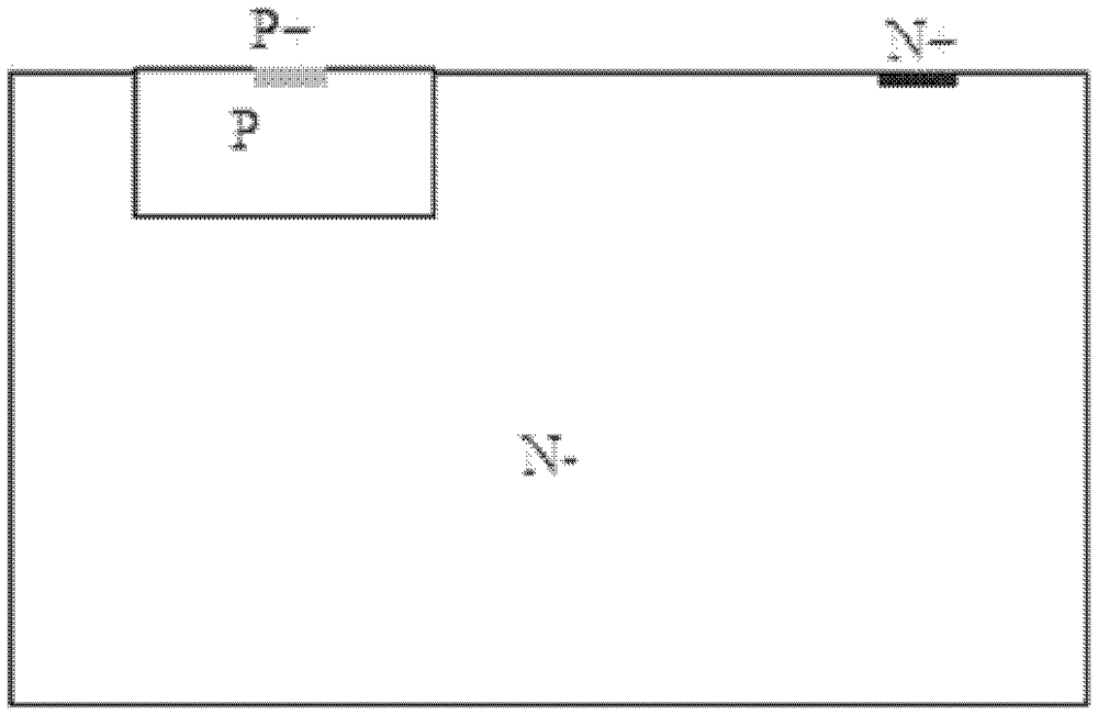
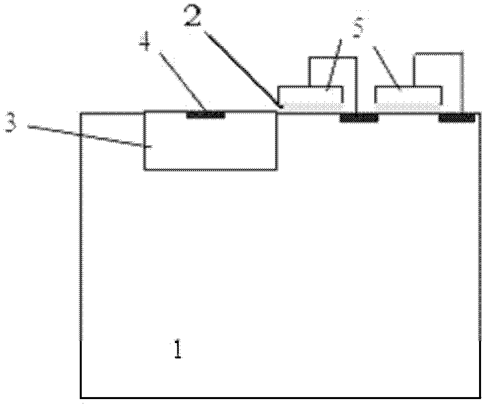
[0031] Such as figure 2 , image 3 As shown, an embodiment of the present invention includes: an N well 3 is formed on the left side of the upper part of the P-type silicon 1, and an N+ injection layer 4 is formed on the upper part of the N well 3; two MOSs connected in series are formed on the upper right side of the P-type silicon 1 structure;

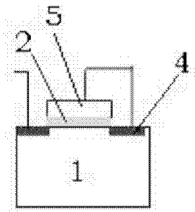
[0032] The MOS structure includes a P-type silicon 1, an N+ injection layer 4, a gate oxide layer 2 and a gate 5; the gate oxide layer 2 is formed on the top of the P-type silicon 1; the N+ injection layer 4 is formed on the top of the P-type silicon 1, and the gate oxide Below the sides of the layer 2; the gate 5 is formed above the gate oxide layer 2;

[0033] Among them, the gate oxide layer 2 of the leftmost MOS structure is adjacent to the N well 3, and the gate 5 of each MOS structure is connected to its adjacent N+ injection layer 4 through metal wires; the P-type silicon adopts the P-type silicon substrate Or P-type silic...


PUM


Abstract

The invention discloses a one-way conductive pressure device with characteristics including: an N well is formed at a left side of an upper part of a P-type silicon and N+ injection layers are formed above the N well; more than two serially connected MOS structures including the P-type silicon, the N+ injection layers, gate oxide layers and gates are formed at a right side of the upper part of the P-type silicon; the gate oxide layers are formed on the P-type silicon; the N+ injection layers are formed at an upper part of the P-type silicon and beneath two sides of the gate oxide layers; and the gates are arranged on the gate oxide layers, wherein a gate oxide layer of a leftmost MOS structure is adjacent to the N well, and the gate of each MOS structure is connected with adjacent N+ injection layers through mental wires. The invention also discloses a manufacturing method for the one-way conductive pressure device The invention also discloses a manufacturing method for the one-way conductive pressure device Compared with traditional high-voltage diodes, the one-way conductive pressure device is capable of providing higher forward-direction conduction current while providing the same breakdown-resistant voltage.

Description

technical field [0001] The invention relates to the field of integrated circuit manufacturing, in particular to a unidirectional conduction withstand voltage device. The invention also relates to a manufacturing method of a unidirectional conductive withstand voltage device. Background technique [0002] The traditional PN junction diode is in a single crystal semiconductor, part of which is doped with acceptor impurities is P-type semiconductor, and the other part is doped with donor impurities is N-type semiconductor, and the transition near the interface between P-type semiconductor and N-type semiconductor The region is called a PN junction, and a space charge layer is formed on both sides of its interface, and a self-built electric field is built. When there is no applied voltage, the diffusion current caused by the carrier concentration difference on both sides of the PN junction is equal to the drift current caused by the self-built electric field, and is in a state ...

Claims


Application Information

Patent Timeline
Patent Type & Authority Patents(China)
IPC IPC(8): H01L27/088H01L21/8234
Inventor 王飞
Owner SHANGHAI HUAHONG GRACE SEMICON MFG CORP
Why Eureka
Try Eureka